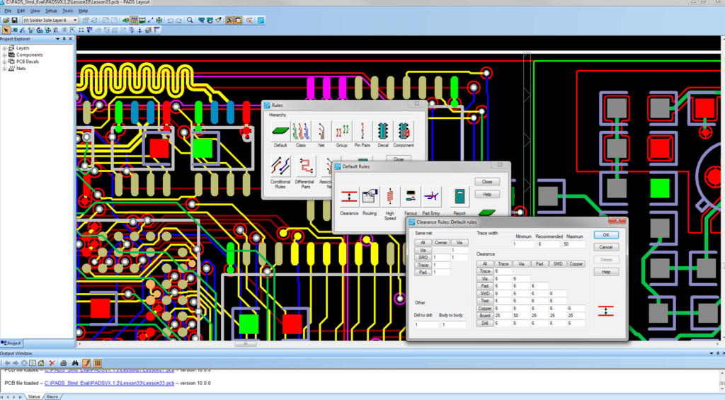
Complex PCB design is an essential aspect of modern electronics. PCBs, or printed circuit boards, are the backbone of electronic devices, providing a platform for the components that make up the device to communicate with each other. PCB design has become increasingly complex over the years, as devices have become smaller and more powerful, and as the demand for higher performance has increased.
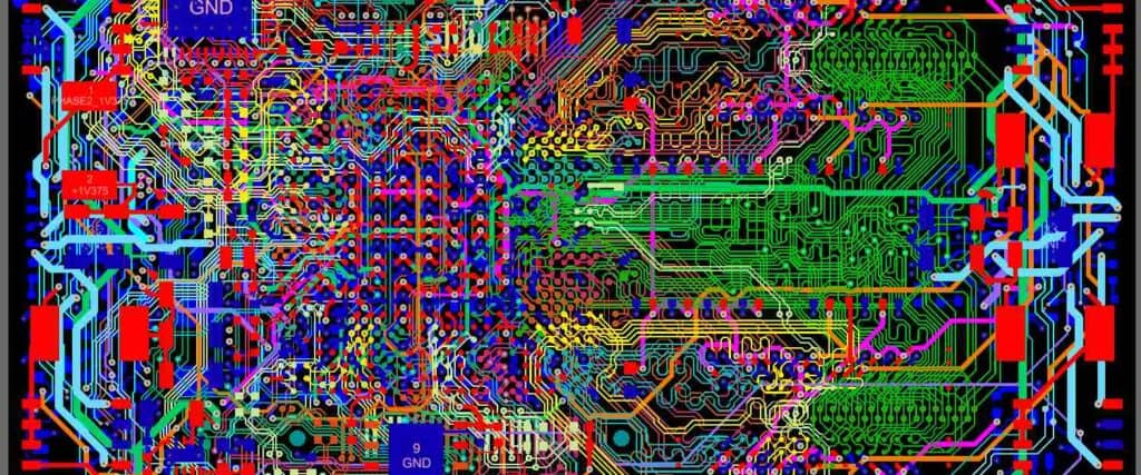
One of the key challenges in complex PCB design is managing the increasing density of components on the board. As devices become smaller, more components need to be packed into a smaller space, which can lead to issues with heat dissipation, signal integrity, and power management. Designers need to carefully consider the placement of components, as well as the routing of traces, to ensure that the board functions as intended. Additionally, designers need to consider factors such as electromagnetic interference (EMI) and electromagnetic compatibility (EMC), which can impact the performance of the device.
Basics of Complex PCB Design
Complex PCB design involves creating printed circuit boards with multiple layers and intricate circuitry. These boards are used in a variety of applications, including aerospace, military, and medical devices. Here are some basics to keep in mind when designing complex PCBs:
-
Layer Stackup: The layer stackup is the arrangement of copper layers, insulating layers, and other materials that make up the PCB. In complex designs, there may be many layers that need to be carefully arranged to ensure signal integrity and minimize noise.
-
Trace Width and Spacing: The width of traces and the spacing between them is critical in complex PCB design. These parameters are determined by the current carrying capacity of the trace, the voltage level, and the required impedance.
-
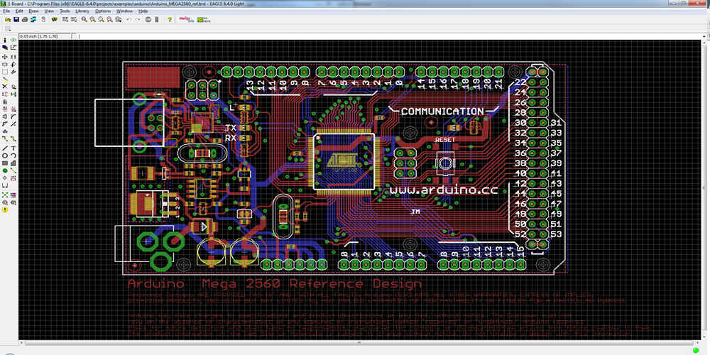
Component Placement: The placement of components on the PCB is important for signal integrity, thermal management, and manufacturability. Components should be placed in a way that minimizes signal interference and allows for efficient heat dissipation.
-
Routing: Routing is the process of connecting components on the PCB with traces. In complex designs, routing can be a challenging task, as there may be many components and tight space constraints. Routing software can be used to automate this process and ensure that the design meets all requirements.
-
Design for Manufacturability: Complex PCBs can be difficult and expensive to manufacture. Designers should keep this in mind when creating their designs and strive to make them as easy to manufacture as possible. This includes using standard components and minimizing the number of unique parts.
By keeping these basics in mind, designers can create complex PCBs that meet all requirements and are manufacturable at a reasonable cost.
Design Considerations for Complex PCBs

Designing a complex printed circuit board (PCB) requires careful consideration of various factors to ensure the board’s functionality and reliability. Here are some important design considerations to keep in mind:
-
Component Placement: Proper component placement is crucial for the board’s functionality and reliability. Components should be placed in a way that minimizes signal interference and reduces the risk of thermal issues. It is also important to consider the assembly process and ensure that components are placed in a way that allows for easy assembly.
-
Signal Integrity: Signal integrity is critical for the proper functioning of a complex PCB. The PCB layout should be optimized to minimize signal interference, crosstalk, and electromagnetic interference (EMI). Careful consideration should be given to the routing of high-speed signals, power planes, and ground planes.
-
Thermal Management: Thermal management is an important consideration when designing a complex PCB. High-power components generate heat, and if not managed properly, can cause the board to fail. Thermal management techniques such as heat sinks, thermal vias, and thermal pads can be used to manage heat and ensure the board’s reliability.
-
Power Delivery: Proper power delivery is essential for the board’s functionality and reliability. The PCB layout should be optimized to minimize voltage drop and ensure that all components receive the required power. Power planes and decoupling capacitors should be used to minimize noise and ensure stable power delivery.
-
Manufacturability: Designing a complex PCB that is manufacturable is essential. The PCB layout should be optimized for the manufacturing process, and the design should take into account the capabilities of the manufacturing equipment. It is also important to ensure that the design meets the manufacturer’s design rules and guidelines.
In conclusion, designing a complex PCB requires careful consideration of various factors such as component placement, signal integrity, thermal management, power delivery, and manufacturability. By keeping these considerations in mind, designers can create PCBs that are functional, reliable, and manufacturable.
Tools and Techniques for Complex PCB Design
Designing complex PCBs requires the use of specialized tools and techniques that can help streamline the process and ensure the final product is of high quality. Here are some of the most commonly used tools and techniques for complex PCB design:
Tools
-
Computer-Aided Design (CAD) software: CAD software is essential for designing complex PCBs. It allows designers to create and edit schematics, simulate circuits, and generate Gerber files for manufacturing.
-
Simulation software: Simulation software can help designers test and verify their designs before manufacturing. It allows designers to simulate how their circuits will behave under different conditions and identify potential issues before they become a problem.
-
3D modeling software: 3D modeling software can help designers visualize their designs in three dimensions. This can be useful for identifying potential issues with component placement and ensuring that the final product will fit within the intended enclosure.
Techniques
-
Design for Manufacturability (DFM): DFM is a set of guidelines that aim to ensure that a design can be manufactured efficiently and accurately. By designing with DFM in mind, designers can reduce the risk of errors and minimize the time and cost of manufacturing.
-
Design for Testability (DFT): DFT is a set of guidelines that aim to ensure that a design can be tested effectively. By designing with DFT in mind, designers can reduce the risk of errors and improve the reliability of the final product.
-
Thermal management: Thermal management is essential for complex PCBs that generate a lot of heat. By using techniques such as heat sinks, thermal vias, and proper component placement, designers can ensure that their designs operate reliably and efficiently.
In conclusion, designing complex PCBs requires the use of specialized tools and techniques that can help streamline the process and ensure the final product is of high quality. By using these tools and techniques, designers can reduce the risk of errors and improve the reliability of their designs.
Advanced Techniques for Complex PCB Design
Designing complex printed circuit boards (PCBs) can be a daunting task, especially when dealing with high-speed signals, high-density boards, and multiple layers. However, with the right techniques and tools, it is possible to achieve a successful design. Here are some advanced techniques for complex PCB design:
1. High-Speed Design Techniques
High-speed signals require careful consideration and planning to ensure a successful design. Some techniques to consider include:
- Using impedance-controlled routing to maintain signal integrity
- Minimizing the length of high-speed traces to reduce signal delay and reflections
- Using differential pairs to reduce electromagnetic interference (EMI)
- Placing decoupling capacitors close to the power and ground pins of high-speed components to reduce noise
2. Thermal Management Techniques
Thermal management is critical in complex PCB designs, especially for high-power applications. Some techniques to consider include:
- Using thermal vias to transfer heat from the top layer to the bottom layer of the PCB
- Spreading out heat-generating components to reduce hot spots
- Placing thermal reliefs on copper pours to improve heat dissipation
- Using a heat sink or a fan to dissipate heat from the PCB
3. Design for Manufacturability (DFM)
Design for manufacturability (DFM) is essential to ensure that the PCB can be manufactured efficiently and cost-effectively. Some techniques to consider include:
- Minimizing the number of drill sizes and hole types to reduce drilling time and cost
- Using standard component footprints to reduce the cost of components and increase availability
- Avoiding complex shapes and angles to reduce the risk of manufacturing errors
- Using panelization to reduce manufacturing time and cost
In conclusion, designing complex PCBs requires careful planning and consideration. By using the advanced techniques mentioned above, designers can achieve a successful design that meets the requirements of their application.
