The ATmega328 is a microcontroller that is widely used in various electronic devices. It is capable of handling multiple tasks and can be programmed to perform a wide range of functions. One of the most important aspects of designing a circuit with an ATmega328 is the PCB layout.
The PCB layout is the arrangement of components on the printed circuit board that connects and controls the microcontroller. A well-designed PCB layout can minimize noise and interference, improve signal integrity, and reduce the risk of errors and malfunctions. To achieve these goals, designers must consider factors such as trace widths, component placement, and power supply routing.
Schematic Design
When designing a PCB layout for the ATmega328 microcontroller, the schematic design is a crucial step that needs to be done with utmost care. A well-designed schematic can ensure that the final PCB layout is accurate and functional.
Components Placement
One of the most important aspects of the schematic design is the placement of components. It is essential to ensure that the components are placed in a logical and organized manner, making it easier to understand the circuit and troubleshoot any issues that may arise.
When placing components, it is also important to consider the physical layout of the PCB. Components that are placed too close together can cause interference, while components that are too far apart can lead to long signal paths and increased noise. Therefore, it is important to strike a balance between component placement and PCB layout.
Power Supply Circuit
The power supply circuit is another critical aspect of the schematic design. The ATmega328 requires a stable and reliable power supply to function correctly. Therefore, the power supply circuit must be designed with care, taking into account the voltage and current requirements of the microcontroller.
One common approach to designing a power supply circuit for the ATmega328 is to use a voltage regulator. The voltage regulator can provide a stable output voltage, even when the input voltage fluctuates. It is also important to include decoupling capacitors in the power supply circuit to reduce noise and stabilize the voltage.
In conclusion, the schematic design is a crucial step in creating a functional and reliable PCB layout for the ATmega328 microcontroller. Careful consideration must be given to component placement and power supply circuit design to ensure the final PCB layout is accurate and functional.
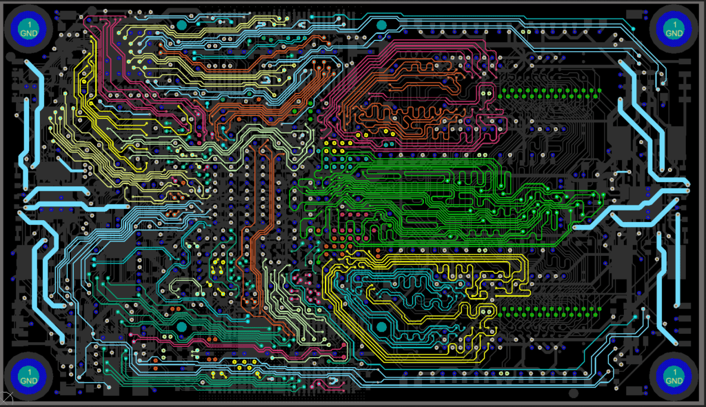
PCB Layout

When designing a PCB layout for the ATmega328 microcontroller, it is important to follow certain guidelines to ensure proper functionality. This section will cover routing guidelines, ground planes, and signal traces.
Routing Guidelines
When routing the PCB, it is important to keep in mind the following guidelines:
- Keep traces as short as possible to minimize noise and interference
- Use wide traces for power and ground lines to reduce resistance and voltage drop
- Keep high-speed signals away from sensitive analog signals to prevent crosstalk
- Use vias to connect traces on different layers of the PCB
Ground Planes
Ground planes are an important part of PCB layout design. They provide a low-impedance path for return currents and help reduce noise and interference. When designing a ground plane:
- Use a solid ground plane on the bottom layer of the PCB
- Connect all ground pins of the microcontroller to the ground plane
- Keep the ground plane separate from other signal traces to prevent interference
Signal Traces
When routing signal traces, it is important to keep in mind the following guidelines:
- Keep traces as short as possible to minimize noise and interference
- Use wide traces for high-current signals to reduce resistance and voltage drop
- Keep high-speed signals away from sensitive analog signals to prevent crosstalk
- Use a series termination resistor for high-speed signals to prevent reflections
By following these guidelines, you can ensure a reliable and functional PCB layout for your ATmega328 microcontroller.
Gerber Files
Gerber files are a set of files that define the PCB layout and design. These files are used by PCB manufacturers to create the physical board. The Gerber files include information about the copper layers, silkscreen, solder mask, drill holes, and other important details.
It is important to ensure that the Gerber files are accurate and complete before sending them to the manufacturer. Any errors or omissions can result in a faulty board. Therefore, it is recommended to use a Gerber viewer to double-check the files before sending them for manufacturing.
Gerber files can be generated using various software tools such as Eagle, Altium, KiCad, and others. These tools provide options to customize the output files according to the manufacturer’s requirements. For example, the manufacturer may require specific drill sizes, layer order, or panelization.
In addition to the Gerber files, manufacturers may also require other files such as the drill file, assembly drawing, bill of materials, and test points. It is important to check with the manufacturer for their specific requirements and guidelines.
Overall, the Gerber files are a crucial part of the PCB design process and must be carefully prepared and reviewed to ensure a successful board manufacturing.
Assembly
Bill of Materials
Before starting the assembly process, it is important to gather all the necessary components and tools. Here is a list of the required components for assembling an Atmega328 PCB:
- Atmega328P-PU microcontroller
- 16MHz crystal oscillator
- Two 22pF ceramic capacitors
- 10k ohm resistor
- 2×3 male header pins
- PCB board
- Soldering iron
- Solder wire
- Diagonal cutter
- Multimeter
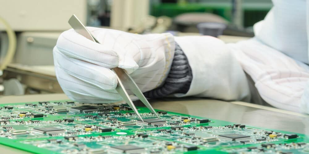
Soldering Techniques
Soldering is a crucial step in assembling an Atmega328 PCB. Here are some tips to ensure a successful soldering process:
-
Clean the tip of the soldering iron before starting. A dirty tip can cause poor heat transfer and lead to unsatisfactory results.
-
Apply a small amount of solder to the tip of the iron to help with heat transfer.
-
Place the component on the PCB board and hold it in place with a pair of tweezers.
-
Heat the pad and component lead with the soldering iron for a few seconds until the solder melts.
-
Apply a small amount of solder to the joint and remove the iron.
-
Check the joint with a multimeter to ensure there is no short circuit or open circuit.
-
Trim the excess component lead with a diagonal cutter.
-
Repeat the process for all components.
By following these tips, you can ensure a successful assembly process for your Atmega328 PCB.
Testing and Troubleshooting
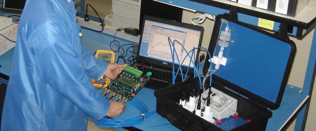
Functional Testing
After completing the PCB layout for the ATmega328, it is important to test its functionality before proceeding with any further steps. The functional testing process involves verifying the proper functioning of all the components used in the design.
One way to perform functional testing is by using a multimeter to measure the voltage levels at various points on the PCB. This can help identify any short circuits or open circuits that may be present. Additionally, using an oscilloscope can help verify the waveform of the clock signal and other signals.
Another important step is to program the ATmega328 with a simple program to test its functionality. This can be done using an AVR programmer and software like AVR Studio or Arduino IDE. Once the program is uploaded, the ATmega328 should be able to execute the program correctly and produce the expected output.
Debugging
If the functional testing reveals any issues, the next step is to debug the PCB layout. One common issue is a short circuit between two or more traces or components. Using a multimeter, the short circuit can be identified and corrected by cutting the trace or removing the component causing the issue.
Another issue that may arise is an open circuit, which can be caused by a broken trace or a faulty component. The multimeter can be used to identify the open circuit and the faulty component can be replaced.
In some cases, the issue may be related to the programming of the ATmega328. In this case, it is important to verify the code and the connections between the ATmega328 and other components.
Overall, testing and troubleshooting are important steps in the PCB design process. By following these steps, any issues can be identified and corrected before proceeding with the final steps of the design.
