What does it mean when someone says that a Copper Coin PCB is being manufactured? Does it mean that a coin is used for the board’s configuration? And what is the reason behind the design?
In this article, we help you understand the meaning of the concept and some of the reasons behind the popularity.
What is the Meaning of Copper Coin PCB?
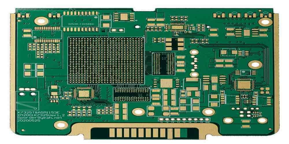
It is a type of Printed Circuit Board (PCB) that has a solid piece of copper added to it. It is worthy of mention that the copper coin circuit board is a type of multilayer board, only that this addition is made.
The other point to note is that the additional or integrated layer of copper foil is used to cover the substrate’s insulating material.
The extra layer is called a coin and it is integrated into the stackup of the multilayer Printed Circuit Board (PCB).
The Evolution of Copper Coin PCB
It is pertinent to mention that this type of circuit board has evolved greatly over the years. It is also a response in line with the ongoing trends and changes in the Printed Circuit Board (PCB) market.
The evolution can be traced back to the earliest 21st century when it became a trend. Since then, newer concepts have been developed to facilitate the integration of Copper Coin PCB concepts into circuit board designs.
Today, we can use it in a wide range of applications. It is therefore important to cite a few important points to note about this type of PCB design.
Heat Dissipation Capabilities
Today, Printed Circuit Boards (PCBs) are not manufactured for the fun of it – or just for facilitating the configuration of consumer electronics.
Now, we need to pay an extra attention to how these circuit boards can be used to facilitate heat dissipation. As heat or excessive thermal energy is one factor that can impede how a circuit board performs.
We are pleased to let you know that it is possible for you to use the Copper Coin PCB to manage heat dissipation. This is possible because of the excellent heat dissipation capabilities, as bolstered by the 400W/m.K thermal conductivity.
Copper Coin circuit boards are often compared to gold, in terms of the heat dissipation capabilities. Although gold can offer up to 5 times the thermal conductivity of copper, it is not often used, due to the costs.
The emphasis on copper usage, therefore, bolsters the provision of heat dissipation with keeping the electrical conductivity.
The thermal conductivity option for Copper Coin PCB is actualized via the direct thermal connection made to the outer layer from one side to the other. It can also be established via a specific layer on the board.
Important Notes About Copper Coin PCB’s Properties
Here are some of the things you need to have in mind before deciding to work with the copper coin circuit board:
- The thermal conductivity of the copper in the Copper Coin PCB is between 30 and 200 times better than the other circuit board’s conductivity materials.
- The thermal conductivity of copper is comparable to any of the popular conductive dielectric prepreg.
- The Copper Coin PCB, once inserted or added to the Printed Circuit Board (PCB) can incorporate or take different configurations or forms.
How Copper Coin PCB Improves Heat Conduction

Considering that most circuit board’s use thermal vias holes for heat dissipation, it became imperative to find an alternative. The previous model, albeit being feasible, doesn’t entirely meet the needed demands for heat dissipation.
The integration of copper into the fold makes it all better due to the excellent heat conduction capabilities. This also goes the extra mile to bolster facilitating or conducting heat from crucial components that the standard via holes wouldn’t enable the thermal energy transfer.
The Types of Copper Coin PCBs
You can find a wide range of configuration options for this type of Printed Circuit Board (PCB). Also, the typologies differ based on the processes used.
Here are some of the common types of Copper Coin PCBs you can find out there:
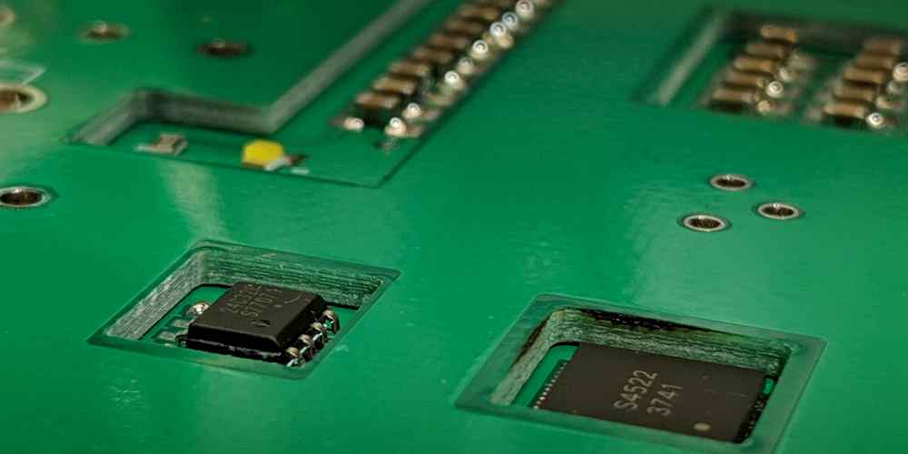
1. Buried Copper Coin PCB
As the name suggests, it has to do with burying or concealing the copper coin inside the PCB. It involves the insertion of a piece of copper, directly under the component. Once placed therein, the circuit board helps to absorb heat and facilitate the dissipation or removal of the same.
Here are some of the factors or properties that make the buried Copper Coin PCB different from the other formats/types:
- The processing power is lower.
- This type of Copper Coin PCB doesn’t cost much money.
Despite the fact that Copper Coin PCBs can facilitate heat conduction, there is a chance that it wouldn’t work as much as expected. That is the case if you were working with the buried Copper Coin PCB.
It is unable to facilitate heat conduction due to the positioning or being buried inside the pre-milling groove.
Despite this inability, a couple of concepts have been developed to facilitate heat conduction with the buried Copper Coin PCB. Some of these processes are:
- The usage of high-thermal conductivity materials.
- Making of denser heat dissipation hole designs.
- Thick copper foil circuit.
2. Embedded Copper Coin PCB
If you are looking to conduct heat faster from a PCB, it has to be with the embedded Copper Coin PCB design. The heat conduction capabilities are enabled via:
- The direct connection of the embedded copper to the inner copper layer.
- The buried Copper Coin PCB facilitates heat conduction in real-time, i.e., as soon as the circuit board is in use.
- It then facilitates heat transfer from the air through the copper coin.
Comparing the Embedded and Buried Copper Coin PCB Technologies
As explained above, there are two major processes for modifying the Copper Coin PCB for improved heat dissipations. These are the embedded and buried formats.
However, the capabilities of the two differ, especially when we put the heat conduction/dissipation capabilities into perspective. For this reason, we want to compare and differentiate between the two:
- Buried Copper Coin PCB is “buried” or kept inside, while the embedded variant is a bit exposed, as it is typically placed where it has a direct connection or “interaction” with the air and the inner copper layer.
- Despite the differences in the heat conduction capabilities, the buried Copper Coin PCB has a significant advantage over the embedded type. The upper hand it has is due to the excellent working capability and reliability, which outshines the difficult process of the embedded Copper Coin PCB.
Advantages of Copper Coin Circuit Boards
If you are unsure of how beneficial this circuit board could be, we have come up with some insider details.
Here are some of the advantages of choosing to work with the Copper Coin PCB:
1. Heat Conduction Plus Control
It is one thing for the copper integrated inside the PCB to facilitate heat dissipation. It is another thing to have a control or be able to regulate how the entire process works.
You can be sure of deriving both benefits with the Copper Coin PCB due to the combination of faster heat conduction and excellent control over the process.
2. High-Speed Communications
You can only say that a circuit board is performing optimally when the speed of conducting heat away from the components in particular and the circuit in general is faster.
With a faster heat conduction capability, you can be sure of using the board in high-speed communication applications. This also extends to the facilitating of high-speed communications between several circuits.
3. Higher Thermal Conductivity
This is the major reason why the board makes heat dissipation faster. A higher thermal conductivity property aids in evening the heat transfer rate.
Where Can the Copper Coin PCBs be Used?
You can use it in the modern electronics. However, have in mind that certain considerations must be made for the best results.
The first consideration is to use the Copper Coin PCB mostly for the high-grade or high-performance-centric electronic devices. These are the devices that require a combination of excellent heat/thermal energy conduction and improved performance.
The second consideration is to use the Copper Coin PCB for the electronic components that have the following provisions:
- Circuit boards with thinner or lighter footprints.
- The electronic components in the targeted devices also need to enable the connection to the Copper Coin PCB either through electrically-conductive tracks or pads.
What is the Way Forward?
Definitely, Copper Coin PCBs are a prayer answered for the proliferation of smaller and lighter Printed Circuit Boards (PCBs). With this proliferation came the need to create adaptable circuit boards that can be used across different markets.
The buried and embedded designs of the Copper Coin PCB help the consumers to have a lot of options to pick from when working on an application.
To crown it all, having a professional circuit board manufacturer that knows how to add the right amount of copper foils makes all the difference. Hillman Curtis is dedicated to helping create the type of electronic device that conducts heat faster and still performs optimally, using the Copper Coin PCB.
