A copper layer in a PCB serves several important functions, from providing a durable surface for traces to helping the device transmit signals. Copper is an excellent conductive material, allowing signals to pass without absorbing electricity. It is also relatively cheap, making copper an excellent choice for PCB manufacturers.
Printed Circuit Boards (PCB) contain the outer and internal layers. They also contain copper, which is incompatible with scoring (V-cut). To ensure compatibility, the mechanical layer of the PCB must include copper markings and a minimum width of 0.5mm.
PCB Layers explained
The copper layer is the first layer on a 2-layer PCB stackup. It is 0.014 in thick, weighs a bit over an ounce, and is the signal layer. Its effect is good on a board with a 0.062-inch final thickness. However, the thickness may vary depending on the parameters used in the board’s fabrication.
The copper layer is an important part of the PCB. It has several functions and is present in different shapes and materials. It helps the board receive appropriate current flow and controls the loss of power on the circuit board. In some cases, copper is present on two sides of the substrate. Experts recommend four-layer PCBs to prevent problems with these electromagnetic effects.
The other three layers of a PCB include ground planes, power planes, and routing layers. The power plane provides the circuit with a clean power source, while the ground plane serves as a common ground for all the components. Finally, the top layer serves as a signal routing layer and connects the components. You can switch this standard 4-layer stack-up depending on the design specifications and the signals on the board.
Inner Layers and Outer Layers
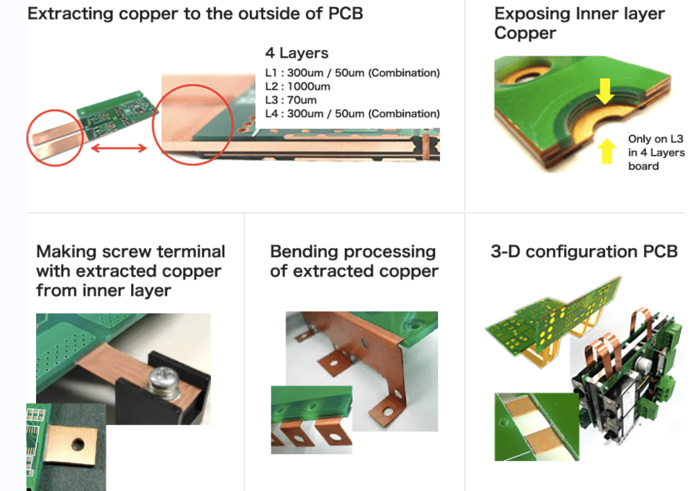
There are two main types of copper on a PCB: the inner and outer layers. Adding an extra layer of copper improves the electrical properties of a PCB while making the board harder to etch. Moreover, it is important to keep the inner layer’s thickness lower than the outer layer’s thickness. The reason for this is that if the thickness of the core is less than the thickness of the outer layers, it may cause see-through gaps. However, this problem can be remedied by increasing the thickness of the substrate. This is a wonderful way to get the PCB layers explained.
The inner layers are conductive. These layers are useful in designing plated holes and pads. You create them using EDA software to define the shape and size of each layer. When designing a multilayer board, you leave a smear of a bonding agent on the surface of the copper layer. To remove this smear, we use a plasma-etch or chemical de-smear process. One does this to ensure a good connection between the copper layers.
Standard Features and Mirroring Issues
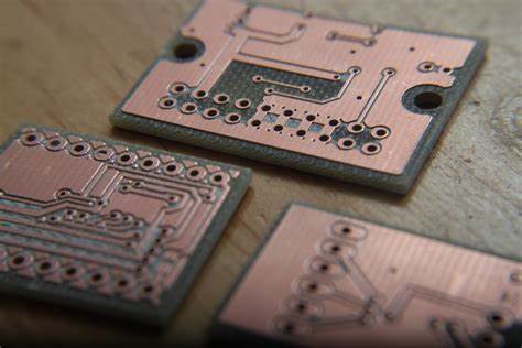
Each copper layer in a PCB begins as a solid sheet of copper. Design files are then photo plotted onto a film and transferred to a resist to protect the copper. After transferring the design file to the panel, the excess copper is etched off by submerging it in a chemical solution.
Copper thickness is typically specified in ounces per square foot. A PCB with a thick copper layer will handle high power. The thickness of a copper layer is generally 1.4 thousandths of an inch or 35 micrometers. You then cover the copper layer with a soldermask layer, which gives the PCB its green color. The soldermask layer also protects the copper traces and prevents solder jumpers.
Another issue that can cause disputes at the final inspection is uneven copper coverage throughout the PCB. This is a common problem, particularly on boards with two-ounce copper and high layer counts.
What functions does the copper layer in PCB offer?
The copper layer in a PCB serves several functions. It is one of several top and bottom layers, each serving a specific purpose. Some PCBs feature a single copper layer, while others feature two copper layers, one on each side of the substrate. Each of these layers provides a different function, and the choice you make is up to you.
Copper is useful in circuits to conduct electrical current and to transmit data. It also contributes to circuit integrity. Different copper weights and thicknesses have different effects on circuit current flow and circuit loss. Copper thickness and quality also impact power plane thermal conductivity and ground plane impedance. Choosing the right thickness and length of copper for your circuit board will help it serve its functions and minimize the risk of solder jumpers.
PCBs can include as many as four copper layers. The top layer serves as the signal layer in multilayer PCBs, while layers 2 and 3 are the ground planes. In multilayer PCBs, we make the copper layer by electroplating copper foil to increase its thickness. The copper thickness is usually adjustable depending on the type of circuit and the type of components.
Choosing the right material for PCB copper
There are several factors to consider when choosing the right material for a copper layer in PCB. One important consideration is the material’s thermal conductivity. We measure thermal conductivity in watts per meter at Kelvin and directly correlates with the heat transfer through a PCB. Most dielectric materials have thermal conductivity rates between 0.3 and 6 W/mk, while copper has a thermal conductivity rate of 386 W/m-oC.
Another important factor to consider is the amount of copper etched away. An over-etched copper layer will expand more than the other layers, resulting in board warping and more catastrophic failure modes. Fortunately, you can take some steps to mitigate this problem.
The temperature at which you assemble the PCB also plays a role in its performance. PCBs can become extremely hot during assembly, and the materials used for the core of the PCB can become brittle. Because of this, PCBs need to have a high glass transition temperature.
Printed Circuit Board and Soldermask Layer
A solder mask is a layer you apply to a Printed Circuit Board before the soldering process begins. You describe the solder mask in a Gerber file. Various types of solder masks exist, including green, black, and transparent/clear soldermasks.
The solder mask layer provides insulation and gives the PCB a green color. It also prevents the solder from jumping over the copper traces. The thickness of the soldermask layer can vary according to the power capacity of the PCB. Therefore, a thicker solder mask layer is better suited for high-power applications.
The Solder mask is an important part of PCB manufacturing. Without it, the solder will not adhere properly. Therefore, you should properly position the solder mask layer on the PCB surface. In addition, it should be large enough to cover the entire PCB surface.
PCB Layers and Copper Traces
When it comes to PCB layers, copper trace width plays an important role. The correct width depends on the copper’s resistance and the pad spacing of the component. It’s important to ensure that the trace width matches the pad spacing to avoid short circuits. The proper trace width will leave enough space for atoms to move freely. As a general rule, trace widths should be six to thirty miles.
Copper balancing, also known as copper distribution, involves ensuring equal distribution of the copper traces throughout each layer. This helps avoid warpage, twists, and bowing. It also minimizes any heat damage that could occur if uneven heating is present. This is done by balancing copper traces within each layer to create a balanced board.
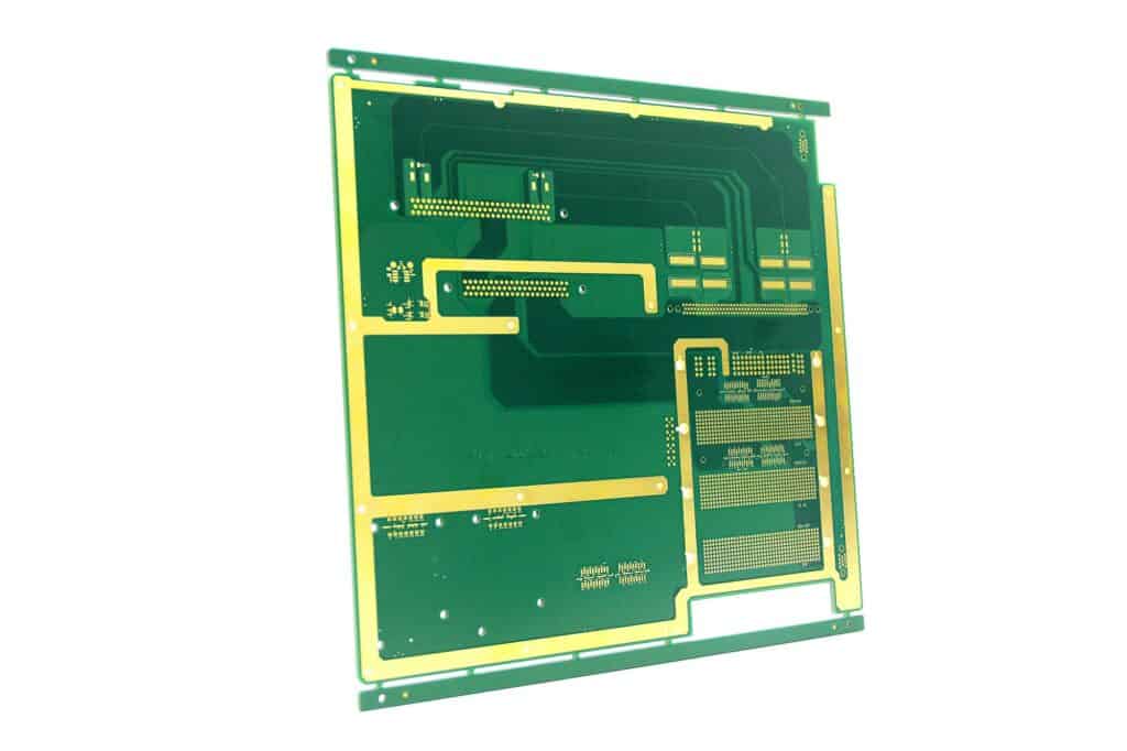
A PCB can be single-sided or double-sided with one copper layer on one side and one on the other. It can also be multi-layered, with layers of copper alternating with layers of substrate. It allows for a greater component density, as the inner copper layers would otherwise take up space between the components. However, multilayer PCBs, with more than two copper planes, make it difficult to change or upgrade the circuits in the field.
Electronic Products and Copper Balancing
The use of copper in electronic products has increased over the past few years. This growth has been driven by the demand for copper in various sectors. The balancing of copper requirements in the different sectors is essential to ensure the supply of copper in the market. The use of copper in electronic products depends on various factors, including its price and quality.
A well-balanced copper layer on a PCB is essential to prevent warping and other defects. Warping in a PCB occurs because of uneven stackups of copper layers on the board. The uneven copper can cause the board to twist during assembly. In addition, it can result from excessive soldering heat, which can bend copper layers. To solve this problem, a PCB CAD design system will automatically add copper pours to sparse areas.
Elsyca PCBBalance simulates different board/panel layouts and compares them to the same-sized copper tracks on the other side. This allows the designer to detect potential plating problems before production begins. Then, the PCBBalance launches a single-click balancing algorithm to define the ideal copper balancing layout. It is integrated into the DFM process and helps engineers achieve a consistent and uniform copper distribution on the board.
Generating output data files for copper layers
There are a few tips to remember when generating output data files for copper layers in PCBs. First of all, you should know the order of the layers. The order is usually unclear from the file names. To clarify this, you can create a PCB Stackup file, which you can include in a Fabrication Drawing or in a separate PDF or Excel file. Another option is to create a mechanical layer and include it in a Gerber file.
Another thing to remember is to avoid generating multiple Gerber files from the same copper layer. Many CAD software packages split the same copper layer into several Gerber files, especially in filled areas. These files will contain separate copper pours, traces, and clearances. This happens because the CAD software has chosen a particular option in its layout software. If this happens to you, check your files with Gerber Viewer to see if you have the correct settings.
Once the copper layer is outlined, you can begin the plating process. This process uses a copper clad FR4 core material. It also includes a peel-off mask applied to one side of the PCB.
Copper Foil and Board Outline
The basic difference between a copper foil and a PCB outline is the copper foil’s surface oxygen content. A copper foil is an insulator that bonds easily to other insulating layers and substrates. The copper foil also provides better continuity of electromagnetic shielding. Therefore, we can use it to cover printed circuit boards themselves.
PCBs have several important advantages over traditional circuit boards. They help eliminate wiring and assembly errors while also improving automation and production labor rates.
Copper foil can be made of two different types, namely, smooth and rough. To determine which type of copper foil you need, ask your vendor for roughness data for their products. This roughness value will help you qualify the material for your design. For example, a copper foil made of reverse-treated foil will have a smooth surface, whereas one that has not been treated will be rougher.
