For months, you may hear about Printed Circuit Boards (PCBs), but you still need to decide if they’re the right fit. Electronics manufacturers have a lot of leeway in terms of how they go about creating their products.
Printed circuit boards (PCBs) should be among your top priorities when designing high-quality electronics. If you’re fine with the value of PCBs and eager to start using one, what’s the best way to start?
This article lists the top PCB manufacturing companies in the industry. These PCB manufacturing firms produce high-quality circuit boards for a wide variety of electronic applications.
There is no doubt that the value these companies bring to the table will help your electronic items stand out from the crowd and sell more than those of your competitors.
First, let’s learn what a printed circuit board is before we look at any specific PCB manufacturer. This method teaches why PCB bare boards are crucial to the electronics industry.
What is a PCB (Printed Circuit Board)?
You’ve heard the term “PCB” bandied about for a while, and its meaning has always eluded you. You care about the logic behind why electrical industry heavyweights like Samsung use circuit boards in their product development processes.
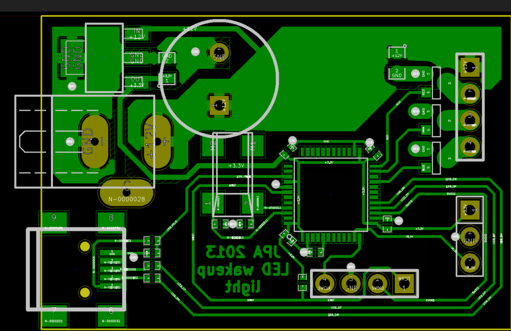
Many others share your inquiries concerning Printed Circuit Boards (PCBs). You must understand that 3mils Printed Circuit Boards (PCBs) are extremely thin boards manufactured and fabricated from laminate materials. Fiberglass and epoxy are the two most common types of laminate that come in handy for making circuit boards.
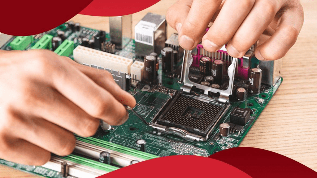
Another critical function of a printed circuit board (PCB) is to serve as the principal medium for connecting the essential elements of electronic devices. In an ideal design, the pads and lines on the circuit board serve as the primary conduit for connecting the relevant electronic components.
The three main electronic components that make up a Printed Circuit Board are:
- Integrated Circuits
- Transistors
- Resistors
PCB Factory Manufacturing Steps
In today’s world, no significant electronic device would function without printed circuit boards (PCBs). All computational electronics, from complex supercomputers to the simplest digital clocks, calculators, and so on, make use of these miraculous innovations.
For the uninitiated, a printed circuit board (PCB) is a piece of equipment that comes in handy to fulfill a device’s electrical and mechanical circuit PCB needs. In a nutshell, printed circuit boards (PCBs) direct the flow of electricity, allowing your electronics to function.
PCBs use a system of copper conductors to distribute electricity evenly across their surfaces. Each part of a PCB has a specific function determined by the intricate network of copper routes. It is how a PCB manufacturer creates printed circuit boards.
Step#1: Design and Output
The PCB layout must be compatible with the circuit board. PCB design tools include OrCAD, Altium Designer, Pads, Eagle, KiCad, etc.
After approval of the production of the PCB layout, manufacturers report the design in a format the manufacturer can read. Popular software is Extensible Gerber. This program can make adorable babies, as did 1980s baby food ads. Gerber is IX274X.
Extended Gerber became the PCB output standard. Gerber files contain copper tracking layers, drill drawings, apertures, component notations, etc., regardless of the PCB design application used to create them. Manufacturers then test the PCB design.
The software uses checksum methods to ensure the final product is error-free. Designers analyze board edge spacing, trace and hole spacing, and hole size.
After inspection, manufacturers transfer the PCB files to fabricators. Almost all PCB Fab Houses undertake a DFM review before fabricating circuit boards to guarantee the design fulfills manufacturing standards.
Step#2: File > Film

After the DFM check and designers output PCB schematic files, manufacturers can produce PCBs. Manufacturers employ plotter printers to make PCB photo films. PCB manufacturers will image the films. This laser printer looks ordinary, yet it has several unusual features. Plotters use high-resolution printing to generate a thin PCB clone.
A black-and-white PCB negative is printed on a plastic sheet. Black ink illustrates the PCB’s inner copper layers. Non-conductive areas are visible in the remaining unobscured part. Clear represents copper, and black represents the etched area. The plotter doesn’t touch the film, and it’s safely hidden.
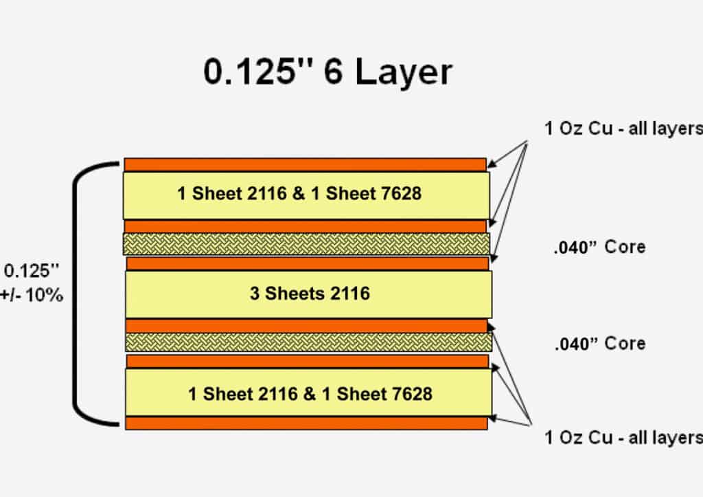
PCB and solder mask layers employ separate transparent and black film sheets. A two-layer PCB requires four sheets for the layers and a solder mask. Every film must match every other film exactly. Together, they can draw a PCB layout schematic.
All films should have registration holes to ensure alignment. Adjusting the film’s location ensures an accurate hole. Manufacturers punch the hole after adjusting the table perfectly. After imaging, the holes then go to the registration pins.
Step#3: Inner Layer Printing
Previous step of film creation aimed at outlining a copper path figure. The next step is to transfer the image from the film onto the copper foil. This phase of PCB production is preparatory to the next. Epoxy resin and glass fiber, commonly known as substrate materials, constitute the basis of the laminate board that is the foundation of a PCB.
It’s perfect for the copper that makes up the PCB to deposit onto laminate. The PCB’s foundation, the substrate, must be solid and dust-proof. Manufacturers ensure that they connect both sides of the copper. The copper must go away to see the pattern from the films.
Next, the clean panel gets photoresist. The photoresist is a coating of UV-hardening photochemicals. This guarantees photo film and photoresist match. Pins hold the films over the laminate panel. Manufacturers now UV blast the film and board.
Light penetrates through the clear coating, hardening the photoresist on the copper. The plotter’s black ink blocks light from reaching regions that shouldn’t solidify; they’ll be removed.
After the board is prepared, an alkaline solution eliminates any unhardened photoresist. A final pressure wash removes any residue.
The final product has copper parts covered with resistance. During this stage, a technician checks the boards for problems. All the resist at this moment represents the PCB’s copper. This phase is for multilayer boards. Two-layer boards skip drilling.
Step#4: Getting Rid of Excess Copper
The board’s next step is to eliminate undesired copper once the photoresist and hardened resist are removed. Just as an alkaline solution eliminates resistance, a stronger chemical eats extra copper. This bath eliminates all exposed copper. Under the hardened photoresist, the necessary copper remains protected.
Copper boards vary. Heavier boards need more copper solvent and longer exposure times. Heavy copper boards demand more track spacing. Most PCBs have similar specs.
Now that the solvent has dissolved the undesirable copper, the preferred copper’s hardened resist must be washed. Another solvent does it. Only the copper PCB substrate remains on the board.
Step#5: Optimal Inspection and Layer Alignment
Clean, ready layers need alignment punches to line up. There needs to be alignment between the Inner layers and registration holes. The technician arranges the layers in an optical punch to correctly punch registration holes.
Once the layers are assembled, manufacturers can’t fix inner layer mistakes. Another machine automatically inspects the panels for flaws. The model is Gerber’s original design.
The machine scans the layers with a laser sensor and compares the digital image to the Gerber file. The technician can view inconsistencies on a monitor if the machine finds inconsistencies. After layer inspection, PCB manufacture continues.
Step#6: Bond and Layer-up
The circuit board is formed. All layers await unification. Once the layers are ready, they must fuse. Now, workers need to join the surface finish. This process involves layering and bonding.
The exterior layer is epoxy-impregnated fiberglass. Manufacturers cover the top and bottom of the original substrate with copper trace etchings and thin copper foil.
Step#7: Drilling
Drilling holes into the stack board is the final step. Precise drill holes are essential for all subsequent components, such as copper via holes and leaded parts. Holes are drilled to a precision of a single hair, with a diameter of 100 microns (the average diameter of a human hair is 150 microns).
Step#8: Copper Deposition
The procedure utilizes chemical deposition to bind the several layers together chemically. The panel is washed in a series of chemicals after meticulously scrubbing.
A chemical deposition method installs a thin coating of copper over the panel during the baths, with an average thickness of around one millimeter. After drilling holes, the copper will be placed inside them.
Step#9: Imaging of the Outer Layer
To begin, we apply a layer of photoresist to the panel and place the layers in a clean environment to ensure that no foreign particles adhere to the surface of the layers. After preparation, the panel enters the yellow room.
The UV rays damage the photoresist. The photoresist is not damaged by yellow light because its wavelength is too short. Transparencies with black ink are affixed to the panel with pins to ensure proper alignment. When a generator shines intense ultraviolet light on a stencil and panel, it cures the photoresist.
Owing to the black ink’s obscuring properties, the unhardened resist on the panel can be safely removed before the panel advances to the next stage.
This procedure represents a reversal from what occurs at the deeper levels. Finally, inspection is performed on the outer plates to confirm that any unwanted photoresist was eliminated during the previous step.
Step#10: Plating
We go back to the plating area. Then manufacturers electroplate a thin coating of copper onto the surface. During the outer layer photoresist stage, copper electro-plating occurs on the panel’s exposed areas.
After the first round of copper plating baths, manufacturers apply tin plating to the panel, which allows for the complete etching of the copper from the board. Tin protects the panel area that needs covering in copper during the subsequent etching process. Manufacturers etch away the panel copper foil in the etching process.
Step#11: The Last Etching
When this happens, the tin shields the valuable copper. The residual resist layer is no more, revealing the copper underneath. Once again, chemical solutions come in handy to dissolve away the surplus metal. At the same time, the tin shields the copper, which is of great value.
Step#12: Applying Solder Mask
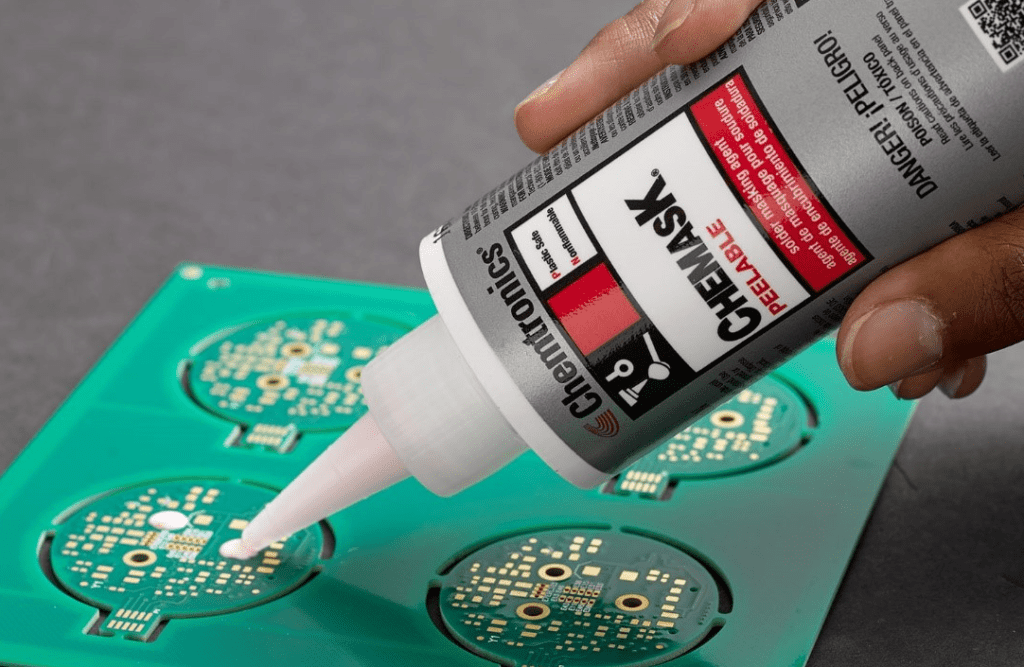
First, manufacturers clean and coat the panels with epoxy solder mask ink before they apply the solder mask to both sides of the board. Then they use a UV light source to expose the boards while a solder mask photo film is in place. The exposed areas haven’t hardened yet, so they’ll be scraped away.
Step#13: Surface Finishing
We chemically treat the PCBs with gold or silver to increase their solderability. During this production process, the pads on some PCBs are additionally flattened using hot air. Using hot air to level the pads ensures they are the same size.
The creation of a finished surface is an outcome of such a procedure. PCBCart can process a wide variety of surface finishes to meet the needs of our diverse clientele.
Step#14: Silkscreen
Ink-jet printing indicates all crucial information regarding the PCB on the nearly finished board’s surface. The printed circuit board (PCB) moves to the final coating and curing phase.
Step#15: Testing
Technicians always double-check their work by running electrical tests on the PCB before calling it good. The automated approach verifies the functioning and design integrity of the PCB.
Using phone probes, we can check the electrical performance of each net on a bare circuit board, a service we term “Flying Probe Testing,” and it’s one we offer here at PCBCart.
Step#16: V-Scoring and Profiling
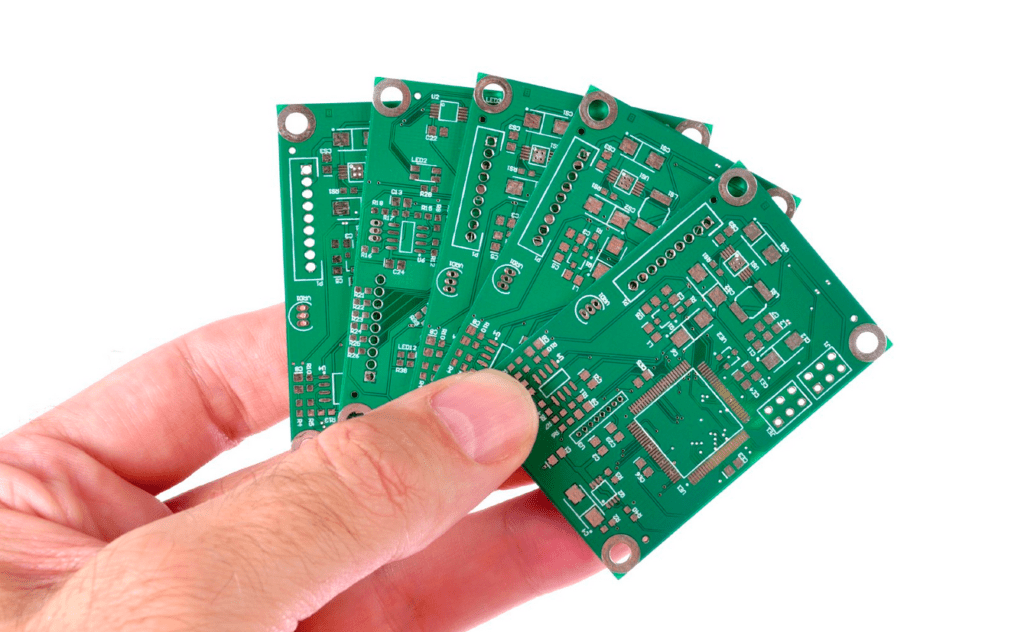
We’re down to the last stage now, and that’s chopping. From a single panel, manufacturers can fashion numerous boards.
A router or a v-groove is the focus of the technique. In contrast to the v-groove, which cuts straight channels along both sides of the board, a router creates tiny tabs along the board’s borders. The boards are removable from the panel in either direction relatively quickly.
The Best PCB Assembly and Manufacturing Services Providers
Since bare circuit boards are vital in electrical device design and production, you need a reliable PCB manufacturer. You must determine whether the PCB company or factory has the expertise and equipment to execute a quality design.
We solved all your PCB design concerns by researching the best PCB manufacturers. Need a bare PCB soon? Here are the leading PCB manufacturers to hire:
1. Hillaman Curtis
Website: https://hillmancurtis.com/
Hillaman Curtis guarantees that it will attend to even the tiniest manufacturing aspects. Their only objective is customer satisfaction with the service they receive.
From intricate multilayer boards to double-sided surface mount designs, they aim to provide the low cost, high-quality PCB products that meet our customers’ requirements.
Their familiarity with IPC Class III standards, strict clean-line requirements, heavy copper, and tight production tolerances enables them to provide our customers and us with precisely what we require.
Hillaman Curtis is the leading PCB manufacturing assembly service due to the real passion of its personnel and the unparalleled technical expertise of its team.
2. Unimicron
Unimicron claims to be the World’s Leading PCB Manufacturer. We cannot disagree, as this PCB maker has continually demonstrated that its motto is accurate.
This circuit board designer’s dedication is unparalleled. In addition to caring about the quality of your circuit boards, they focus on accelerating the PCB manufacturing and production process.
This PCB manufacturer is no longer conducting business as usual. More than waiting and less spending than your planned amount.
3. DSBJ
Printed Circuit Boards (PCBs) come in handy in various economic sectors. From industries to Artificial Intelligence (AI), circuit board demand continues to rise.
Only a few PCB producers know the additional opportunities for diversification and staying relevant in the PCB business. However, DSBJ knows how which is why it is one of the greatest PCB makers around.
This PCB company has continuously grown over the past 32 years, incorporating innovations and ideas to improve their design, quick turn PCB prototype, and manufacture of circuit boards.
4. Zhen Ding Tech
Zhen Ding Tech must be the most well-known PCB maker due to the superior quality of its products. This manufacturer of circuit boards feels that the future would be unlocked more if there were sufficient materials to aid the creation of circuit boards.
Zhen Ding Tech has been in the headlines over the past few years as one of the circuit board manufacturer that mix the Internet of Things (IoT), 5G Technology, the Internet of Vehicles, and Artificial Intelligence to offer a variety of customized solutions.
Zhen Ding Tech simplifies the circuit board manufacturing process by isolating its essential component.
5. Shennan Circuits
Shennan Circuits is not your typical PCB manufacturer that accepts orders and creates Printed Circuit Boards (PCBs).
Instead, this circuit board designer has consistently adapted and incorporated new design trends into its circuit board design manufacturing capabilities.
In the thirty years since its founding in 1984, Shennan Circuits has expanded its services to four locations in China and developed subsidiaries in North America. This PCB maker has also mentioned European Research and Development (R&D) facilities as part of their goal of being an industry leader.
By its mission to be a “world-class supplier of electronic circuits technology and solutions,” this PCB maker has performed admirably.
Conclusion
Hundreds of Printed Circuit Board (PCB) manufacturers exist, as you, no doubt agree. Only some, however, of these manufacturers can confidently promise the timely completion of excellent work without sacrificing quality and familiarity with emerging PCB industry trends.
We’ve gone ahead and completed the project for you. You can find the top designer by going through these PCB manufacturers’ guides. I hope this article was of help to you in knowing the best PCB Soldering services providers. Here, I conclude my article. For more informative articles, stay tuned.
