When selecting a PCB assembly company, there are several factors to consider. These factors include how much the work will cost per unit and whether you want extra testing or other services. Naturally, the more advanced the project is, the higher the labor cost is likely to be. However, you can reduce the cost per unit by supplying your components.
NexusPCB Technologies
NexusPCB Technologies is a company founded in 2015, and it manufactures printed circuit boards, cable assemblies, and harnesses. They serve consumer electronic components, medical devices, instrumentation, and aerospace industries. The company also provides material testing.
The company’s PCB assembly services are suitable for small and large-scale production runs. They offer a quick turnaround time and no minimum order quantity. Their PCB assembly services are available to various industries, and they have expertise in all three types of mixed assembly. They can manufacture rigid, flexible, and mixed boards.
The company’s skilled human resources, advanced technologies, and relevant certifications enable them to produce high-quality products. They are in West Chicago, Illinois. Their military PCB assembly services include production-type, single-sided, and high-density PCBs.
Another leading PCB assembly manufacturer is Advanced Circuits. Founded in 1996, Advanced Circuits has been the leader in the PCB industry. As one of the largest PCB manufacturers in the US, they strive to deliver innovative PCB technology. They also maintain the highest quality standards in the industry. The company manufactures PCBs for DOD contracts in the United States. They produce PCBs with advanced features that can deliver exceptional reliability, precision, and robustness.
These companies are the cream of the PCB assembly industry. However, each has a distinct specialty and offers a wide range of services. Therefore, choosing a top-rated PCBA manufacturers that can provide the best quality PCB for your product is essential.
Technical Manufacturing Corp.
If you are looking for a contract electronics manufacturer, you have probably come across the name Technical Manufacturing Corp. Whether it is a printed circuit board, circuit card, or optical test bench, Technical Manufacturing has a solution to meet your needs. The company is headquartered in Peabody, MA, and has an estimated $30 million annual sales.
In response to customer demand, the company has expanded its manufacturing facility for the fourth time in the last 15 years. The expansion centers around a new welding facility and a larger assembly area. As a result, the company’s products are helpful in the semiconductor, photonics, and life science industries. In addition, the company’s innovative vibration isolation systems can prevent the effects of noise on sensitive instruments.
Hitech Circuits
Hitech Circuits is a company based in Shenzhen, China, offering a comprehensive array of electronic components manufacturing services, including PCB assembly and prototyping. The company specializes in high-density interconnection (HDI), flexible and rigid printed circuit boards, and special process PCBs. In addition, Hitech provides one-stop and full-service mixed assembly and electronics manufacturing services and PCB testing services.
PCB assembly is a complex process requiring years of experience and precision Zero-Defect manufacturing. Unfortunately, not every PCB assembly service provider can meet this demanding standard. Therefore, you should choose a reliable company that can deliver your orders within five to eight working days.
PCBWay
PCBWay is another leading PCB manufacturer and assembly company with complete PCB manufacturing services. The company is a one-stop shop for PCB assembly and prototyping and has a team of professionals with decades of experience. In addition to PCB assembly, PCBWay offers a broad range of PCB services, including custom PCB design and manufacturing, PCB prototyping, and other custom electronics needs.
Excello Circuits
PCB assembly is difficult and requires years of experience and precision Zero Defect. Not all PCB assembly service providers can meet these standards. Those who work with OEMs and Contract Manufacturers cannot afford to have margin errors. The following are some of the top PCB assembly companies in the USA.
Excello Circuits is a PCB assembly company located in Phoenix, Arizona. The company manufactures and assembles custom circuit boards for companies around the world. Their PCB assembly services include all stages of the PCB manufacturing process, including PCB design, layout, and PCB manufacturing.
Saturn
Saturn was founded in 1985 by Nagji Sutariya and two nephews. Since the start, they have focused on quality. They have learned from their mistakes and have since been one of the top domestic PCB assembly companies. They have invested in new PCB technology and manufacturing process to ensure their customers receive the highest quality products.
Advanced Circuits, Inc.
This PCB assembly company in Aurora, CO, has over 500 employees. This company specializes in small-run PCBs and offers a PCB prototyping program for engineering students. IndustrySelect: IndustrySelect is an online database of 460,000 industrial companies, including printed circuit board manufacturing companies.
Transline Technology, Inc.
The vision of Transline Technology lies in partnering with visionary engineers and businesses from various industries to design and manufacture circuit boards. We pursue the most advanced technologies in the industry while still adhering to tried-and-true PCB manufacturing practices. We work with our customers to deliver superior quality and reliability from the design phase to the end product.
The company focuses on RF-printed circuit boards, which account for 60 percent of its overall sales. In addition, HI Electronics provides products for the RF/microwave industry, including RF shielding and solder paste masks for assembly. While Transline has limited rigid-flex capability, the new acquisition will expand its capabilities in this area. HI, Electronics has focused on the automotive, computer, and aerospace industries in the past, but this acquisition will allow them to serve the RF/microwave markets more broadly.
Request a free copy to obtain a Transline Technology, Inc. credit report. You can see the business’s credit score, payment history, court judgments, ownership structure, and up to five years of financial statements. The company has seven employees in total. For more information, you can visit their website.
Transline Technology, Inc. designs and manufactures circuit boards for the Microwave, RF, and High-Performance markets. With over 20 years of experience in the field, the company can handle even the most complex design challenges. With its in-house manufacturing and quality control, Transline has earned a loyal following. In 1996, Transline relocated from Glendale, California, to Anaheim, California, where it now operates from its headquarters. In addition, the company has a 20,000-square-foot facility near Disneyland.
Thomas Instrumentation, Inc.
Founded in 1971, Thomas Instrumentation, Inc. is in Cape May Court House, New Jersey. It primarily operates in the Computer Peripheral Equipment, NEC sector. It currently employs ten people at its Cape May Court House branch location. In addition, the company engages in manufacturing activities at this facility.
Thomas Instrumentation is a full-service electronics design and manufacturing company that can customize solutions for any need. The firm offers engineering, manufacturing, overhaul, testing, and other services. It is an award-winning supplier of flight controls, accessory systems, and winch systems. It also specializes in ball screws and servo design. The company serves both prime and direct markets. It is certified to the AS9100 Rev.C quality standard.
PCB Assembly services Process Steps
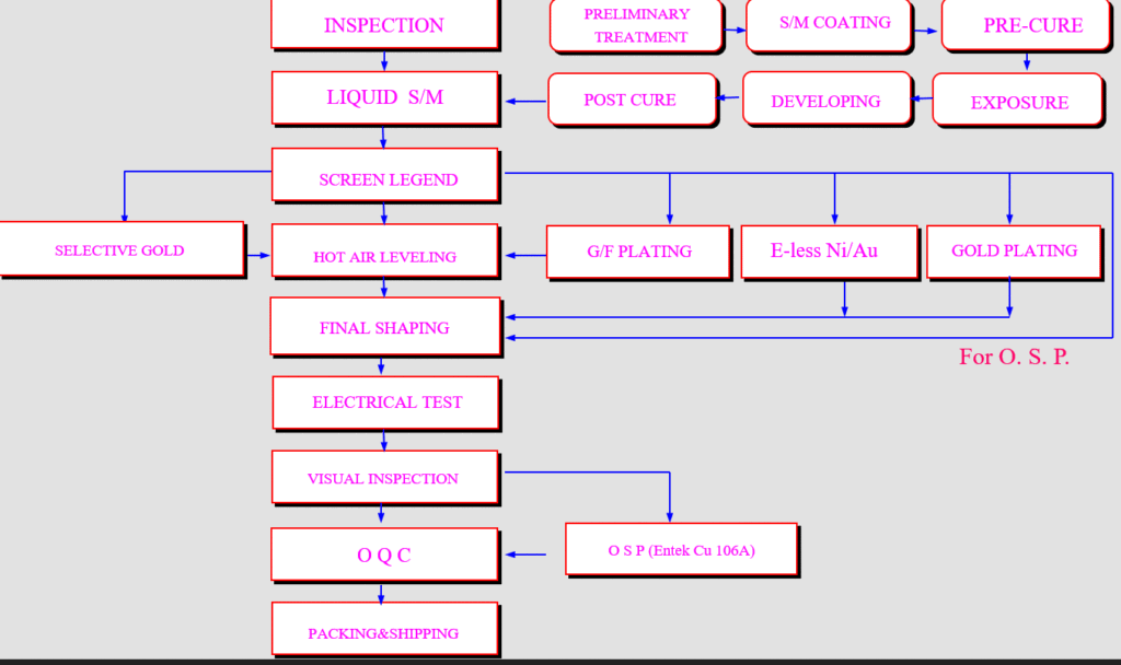
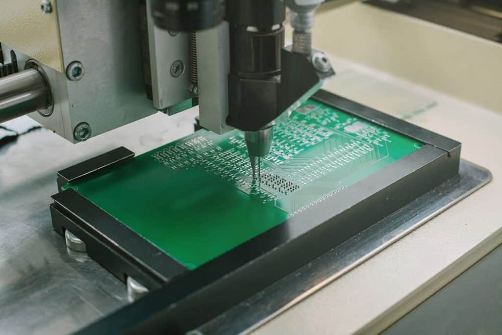
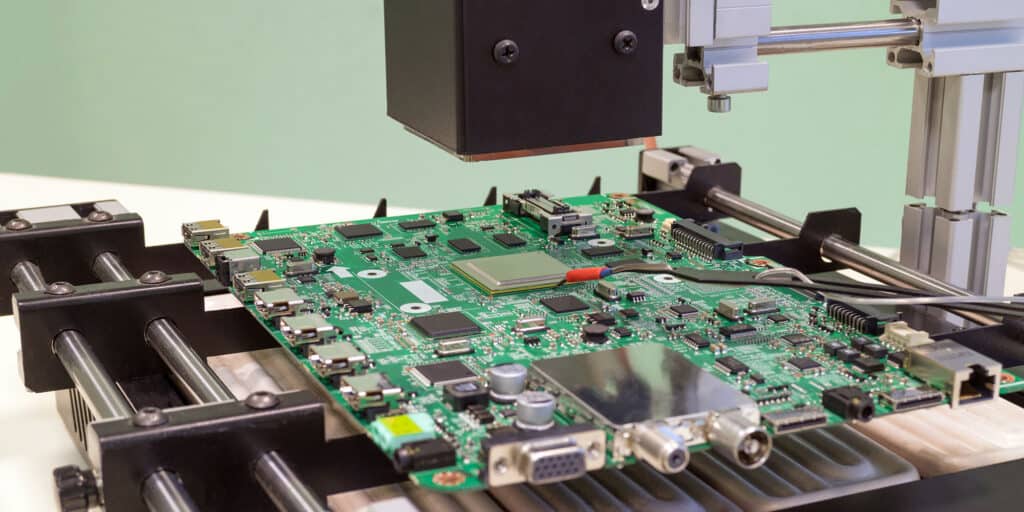
PCB Assembly is a multi-step process that starts with receiving the PCB panels and ends with soldering. This process involves applying solder paste with a stencil or squeegee to the PCBs. They then assemble the PCB panels. Next, they are ready to be tested. AOI or PCB placement machines help to make these boards. Gerber or CAD data is necessary for this process.
Creation of Electrical Circuits in Outer Layers
Electricity, also known as electric current, is a flow of charged particles from a place of higher potential to a place of lower potential. This flow is similar to water flowing downhill as it follows the path of least resistance. To generate electricity, a device must collect electrons and provide a path for them to flow. A nylon carpet, for example, can act as a capacitor for the electrons and create a spark or small shock.
The conductive materials used in printed circuits are copper, silver, or gold. The copper is either plated or etched away to create the desired pattern. The copper is then coated with tin-lead to resist oxidation. The contact fingers of these devices are gold or nickel-plated. In addition, purchased components are used, including capacitors, diodes, transistors, and integrated circuit chips.
PCBs consist of multiple layers, which connect using vias. Vias are holes in the layers that allow electrical signals to flow. The precision of drilling is an essential factor in determining the quality of PCB manufacturing. By evaluating the quality of each component, you can choose which material is best for your application.
Similarly, the transistors consist of p and n-type transistors. These transistors have two types of terminals, the emitter, and the collector. P-type transistors contain a p-type silicon base and two n-type silicon slabs. The emitter emits carriers while the collector collects them.
Solder paste stenciling
Solder paste stenciling is a critical step in the PCB assembly process. It ensures that the solder paste deposited on the PCB stays in the holes. Several factors affect the stenciling process. First, they remove the speed at which the stencil is essential. They must remove the stencil at a speed that does not cause the solder paste to withdraw from the apertures. Generally, this speed should be about three millimeters per second. Any faster than this, the paste will fail to release from the apertures and leave high edges on the board.
Another essential factor to consider is the size of the stencil. The stencil needs to be smaller than the size of the PCB pad. It should also cover at least two-thirds of the area of the PCB pad. Choosing a suitable stencil will significantly affect the flow of solder paste printing on the PCB.
Chemical etching
The PCB assembly process often involves chemical etching. Chemical etching involves exposing the board to a chemical that eats away the exposed copper. The process is usually speedy but can be expensive. In addition, they must specify the chemical used for the particular application. It can also damage the board if left too long. In addition, there are several variables to consider, such as the rate at which the layers move and the amount of copper that is etched.
PCB assembly begins by designing and printing the inner layers of the circuit board. Then they cover the layers with thin copper foil. Once the inner layers are ready, the board is ready for etching.
Solder paste application
Solder paste is a substance used in the soldering process. It is a mixture of metals and fluxes. The viscosity of the paste varies depending on its metal content. When soldered at high temperatures, the paste’s viscosity decreases. Moreover, solder paste can become deformed if stored at low temperatures. Hence, they must perform solder paste storage in a clean environment.
Solder paste application depends on stainless steel, Mylar, or polyimide stencils. The size of the stencil is a critical factor governing the amount of solder paste that is applied. Thinner stencils are used for 0603 capacitors and 0.05″ resistors, while thicker stencils are ideal for larger devices.
Reflow soldering
Reflow soldering is a critical process step that requires careful preparations. During this step, the PCB is heated to a specific temperature to melt the solder paste. Once the paste melts, the PCB cools down naturally. There are several different types of solder paste. For the best results, it’s essential to use the right one for your particular needs. If you’re unsure which one to use, consult your supplier or perform a trial run.
Reflow soldering is typically a time-consuming process. Therefore, it is ideal for circuit boards that do not contain many electrical components. However, paying close attention to the solder joints is essential, as they need to be shiny and fill the copper pad. In addition, the solder paste must be kept at a high enough temperature to reach its melting point without causing the component to break.
Cleaning PCB assembly residues
PCB assembly processes can leave residues and contaminants on the board, which can affect the reliability of the finished board. Although these residues can be difficult to identify, they can cause problems during testing. Additionally, these contaminants can pose a bigger threat over the long term, as they can reduce the reliability of the finished board. Therefore, it is vital to clean PCB assembly processes to avoid these problems properly.
We must remove PCB assembly residues before reworking or soldering. Lead-free soldering requires higher temperatures and highly activated fluxes, which may require more time and aggressive cleaning methods. Depending on the board’s level of aqueous flux residues, extra agitation and a stronger solvent may be necessary for complete removal. Moreover, a circuit board manufactured with a blend of different methods may be more challenging to clean because the residues are thick and sticky. Further, thick flux residues may create flux dams, making it difficult to access components with standoffs.
Surface Mount Technology in PCBA
In PCBA, surface mount technology helps reduce components’ physical size. As a result, this technology can increase the density and functionality of ICs and memory components. During the surface mount assembly process, components are placed on a mating surface so that the pin distances between the components are between 0.3 mm and 0.635 mm.
Surface mount technology is an increasingly common way to place components on a PCBA. The resulting smaller package size allows for easier assembly and increased circuit densities. It also allows for smaller circuit boards, machines, and subassemblies. However, it’s essential to choose a surface mount company carefully.
Surface mount technology is also popular for the applications of power semiconductors. It allows engineers to easily install the components on the board by applying them directly onto the surface. This type of assembly also enables automation of the manufacturing process, which can save time and money. The technology also allows more components to be installed on the same board, thereby increasing its usability.
In the electronic industry, SMT is one of the most common technologies. It allows electronic components to be mounted without drilling, making them smaller and lighter than their through-hole counterparts. It can also help improve routing density, meaning we must drill fewer holes to install the components.
PCB Substrate Materials
The most common PCB substrate type is FR4 (glass-reinforced epoxy laminated sheet). It is a water-resistant and flame-retardant material. In addition, FR4 has a high glass-transition temperature and tensile strength, making it an excellent choice for rigid PCBs. It is also the most cost-effective material used for PCBs nowadays. Alternatively, you can choose FR-2, a type of FR4 substrate that consists of phenolic material.
This material has a long history in the electronics industry. The technology used to make it has evolved from the earliest days to the present. The rapid expansion of PCB products has spurred the development of PCB substrate materials. Today, the PCB industry has diversified into various types of multilayer PCBs.
One type of PCB substrate material is copper-clad laminate (CCL). It is made from copper-covered foil and completed by a thin adhesive. Its thickness is generally 1.0mm to 2.0mm. PCB manufacturers use this material to produce high-quality, reliable printed circuit boards. In addition, it has a low-temperature sensitivity, making it ideal for multilayer PCB fabrication.
Thermal conductivity is another factor to consider when choosing PCB substrate materials. While most PCB substrate materials have a thermal conductivity of 0.3 to 0.6 W/MoC, copper is far more thermally-conductive at 386 W/MoC. Therefore, copper plane layers will take away more heat than dielectric materials. This factor is critical when considering impedance, signal integrity, and high-frequency electrical performance.
The Permanent Interconnection of Layers in PCB manufacturing
PCB assembly involves the permanent interconnection of layers. The process involves creating a hole in the top layer that connects to the conductor on the next layer. For this, we drill a clearance hole into the assembly. Next, the hole is filled with solder to complete the interconnection.
The PCB assembly process is complex and requires careful consideration of several elements. As a result, even small changes in the procedure can significantly affect the cost and quality of the final product. The following process descriptions provide an overview of typical PCBA technologies and procedures. However, the manufacturing process depends on specific customer requirements and design files.
The process of the PCB assembly line consists of several manual and automated steps. You can choose between manual and automated processes, and we will walk you through each step in this article. In general, the board consists of a copper foil layer. This layer can connect the layers of the PCB.
PCB assembly companies require the design file of the PCB to perform the process. The assembly team checks the design for problems, including redundant or missing components. Gaps between components on a PCB can result in shorts, malfunctions, and other issues. Therefore, having a suitable design file is essential to avoid these problems.
