PCB design layout is a crucial aspect of electronic product development. It involves designing the physical layout of the printed circuit board that connects and controls the various electronic components of a device. The layout of a PCB can significantly impact the performance, reliability, and manufacturability of an electronic product.
The design layout of a PCB must take into account various factors, including the size and shape of the board, the number and type of components, and the electrical and thermal properties of the circuit. A well-designed PCB layout can minimize signal interference, reduce power consumption, and improve the overall functionality and efficiency of the device. Additionally, a well-designed layout can simplify the manufacturing process, reduce costs, and improve the reliability of the final product.
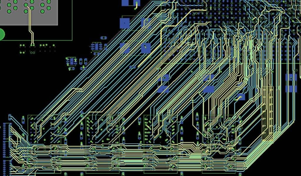
Basics of PCB Design Layout
PCB design layout is the process of arranging components and traces on a printed circuit board (PCB) to ensure optimal functionality and performance. It is an essential step in the design and manufacturing of electronic devices and systems.
The following are some basic considerations to keep in mind when designing a PCB layout:
-
Component placement: Components should be arranged in a logical and efficient manner to minimize the length of traces and reduce the risk of interference and noise. Components that are sensitive to noise should be placed away from noisy components.
-
Trace routing: Traces should be routed to minimize their length and ensure that they can carry the required current without overheating. Traces should also be arranged to avoid crossovers and minimize the risk of interference and noise.
-
Ground planes: Ground planes are large areas of copper that are connected to ground and used to provide a low-impedance return path for signals and to shield against interference. They should be placed on the same layer as the signal traces and connected to the ground pin of each component.
-
Power planes: Power planes are large areas of copper that are used to provide a low-impedance power distribution network for the components. They should be placed on a separate layer from the signal traces and connected to the power pins of each component.
-
Signal integrity: Signal integrity is the ability of a signal to maintain its quality and integrity as it travels through the PCB. It is affected by factors such as trace length, impedance, and termination. Signal integrity should be carefully considered during the design process to ensure optimal performance.
In summary, PCB design layout is a critical step in the design and manufacturing of electronic devices and systems. Proper component placement, trace routing, ground planes, power planes, and signal integrity considerations are essential to ensure optimal functionality and performance.
PCB Design Layout Process

The PCB design layout process involves several steps that ensure the successful creation of a printed circuit board. Here are the steps involved in the process:
-
Schematic Capture: This step involves creating a schematic diagram of the circuit design using a software tool. The schematic diagram shows the components and their connections.
-
Component Placement: In this step, the components are placed on the PCB layout based on their connectivity and functionality. The placement of components should be done in a way that minimizes the length of the traces and the number of vias.
-
Routing: This step involves connecting the components on the PCB layout using copper traces. The routing process should be done in a way that minimizes the length of the traces and the number of vias.
-
Design Rule Check (DRC): This step involves running a DRC to check the PCB layout for errors such as clearance violations, overlapping components, and other design rule violations.
-
Gerber Generation: The Gerber files are generated from the PCB layout, which are then used to create the PCB.
The PCB design layout process is critical to the success of any electronic project. By following these steps, you can create a functional and reliable printed circuit board.
PCB Design Layout Tools
When it comes to designing a printed circuit board (PCB), having the right tools is essential. There are several software options available to help with PCB design layout, each with its own set of features and capabilities. Some of the most popular tools include:
-
Altium Designer: This software offers a comprehensive set of tools for PCB design, including schematic capture, PCB layout, and 3D visualization. It also includes features for design rule checking, signal integrity analysis, and more.
-
Eagle PCB: Eagle PCB is a widely used software for PCB design, offering a user-friendly interface and a range of features. It includes a schematic editor, layout editor, and autorouter, as well as support for importing and exporting files in various formats.
-
KiCad: KiCad is an open-source software suite for electronic design automation (EDA), which includes tools for schematic capture and PCB design. It offers a range of features, including 3D visualization, design rule checking, and more.
-
PADS: PADS is a PCB design software from Mentor Graphics, offering a range of tools for schematic capture, layout, and verification. It includes features for signal integrity analysis, thermal analysis, and more.
Overall, the choice of PCB design layout tool will depend on your specific needs and preferences. It’s important to consider factors such as ease of use, cost, and available features when selecting a tool for your project.
Design Rules and Constraints
Design rules and constraints are essential considerations when designing a printed circuit board (PCB). These rules and constraints ensure that the PCB design is manufacturable, functional, and reliable.
To ensure manufacturability, PCB designers must follow specific design rules. These rules define the minimum width and spacing of traces, the minimum clearance between copper features, and the minimum size of drill holes. By following these rules, designers can ensure that the PCB can be fabricated without errors or defects.
In addition to manufacturability, designers must also consider functional and reliability constraints. These constraints define the electrical and mechanical requirements of the PCB. For example, the maximum current that a trace can carry, the maximum voltage that a component can withstand, and the maximum temperature that the PCB can operate at. By following these constraints, designers can ensure that the PCB functions correctly and reliably.
PCB design software often includes a design rule checker (DRC) that verifies that the design meets the specified rules and constraints. The DRC can detect errors such as overlapping traces, clearance violations, and unconnected nets. By using the DRC, designers can identify and correct errors before manufacturing the PCB.
In conclusion, design rules and constraints are critical considerations when designing a PCB. By following these rules and constraints, designers can ensure that the PCB is manufacturable, functional, and reliable.
Signal Integrity and Power Integrity Considerations
When designing a PCB layout, signal integrity and power integrity are two critical factors that must be taken into consideration. Signal integrity refers to the ability of a signal to travel from the source to the destination without any distortion or loss. On the other hand, power integrity refers to the ability of the power supply to provide a stable and noise-free voltage to the components on the board.
To ensure signal integrity, the following considerations must be taken into account:
-
Trace Length: The length of the traces should be kept as short as possible to reduce the chances of signal distortion and interference.
-
Trace Width: The width of the traces should be selected based on the amount of current they are expected to carry. Wider traces can carry more current without overheating.
-
Ground Planes: A solid ground plane can provide a low-impedance return path for the signals, reducing the chances of noise and interference.
-
Termination: Proper termination of high-speed signals is critical to prevent signal reflections and ringing.
To ensure power integrity, the following considerations must be taken into account:
-
Decoupling Capacitors: Decoupling capacitors should be placed as close as possible to the power pins of the components to provide a low-impedance path for high-frequency noise.
-
Power Planes: A solid power plane can provide a low-impedance path for the power supply, reducing the chances of voltage drops and noise.
-
Power Supply: The power supply should be carefully selected to ensure that it can provide a stable and noise-free voltage to the components.
In conclusion, signal integrity and power integrity are critical factors that must be taken into consideration when designing a PCB layout. By following the above guidelines, designers can ensure that their designs are robust and reliable.
Design for Manufacturing and Assembly (DFMA)
Design for Manufacturing and Assembly (DFMA) is a methodology that aims to optimize the design of a product to make it easier and more cost-effective to manufacture and assemble. DFMA is an important consideration in PCB design because it can help reduce the time and cost of producing a product.
DFMA involves two primary steps: Design for Manufacturing (DFM) and Design for Assembly (DFA). DFM focuses on designing the product in a way that is easy to manufacture, while DFA focuses on designing the product in a way that is easy to assemble.
DFM involves considering factors such as the choice of materials, the size and shape of the product, and the manufacturing process itself. By designing a product with these factors in mind, it is possible to reduce the time and cost of manufacturing.
DFA involves considering factors such as the ease of access to components, the use of standard parts, and the orientation of parts. By designing a product with these factors in mind, it is possible to reduce the time and cost of assembly.
In PCB design, DFMA can be achieved through the use of techniques such as panelization, which involves designing multiple PCBs on a single panel to reduce manufacturing costs, and the use of standard components, which can reduce the time and cost of assembly.
Overall, DFMA is an important consideration in PCB design because it can help reduce the time and cost of producing a product. By designing a product with manufacturing and assembly in mind, it is possible to produce a high-quality product that is both cost-effective and efficient to produce.
