PCB design is an essential aspect of electronics engineering. It involves creating the layout of a printed circuit board that connects electronic components to form a functional device. PCB design can be a complex process that requires precision and accuracy to ensure the final product functions correctly. Fortunately, there are many software tools available to help engineers design PCBs, and Fusion 360 is one of them.
Fusion 360 is a popular software tool that is widely used for 3D modeling and product design. It is also an excellent tool for designing PCBs. With its intuitive user interface and powerful design capabilities, Fusion 360 makes it easy for engineers to create complex PCB layouts quickly. The software comes with a range of features that enable users to create custom components, import schematics, and generate 3D models of their designs. Whether you are a beginner or an experienced PCB designer, Fusion 360 offers a range of tools and features that can help you create high-quality PCB designs.
Creating a New PCB Design
Setting Up the Project
To start designing a new PCB in Fusion 360, you first need to create a new project. Go to the “File” menu and select “New Project”. Give it a name and select “PCB” as the project type. Once you have created the project, you will be prompted to create a new design.
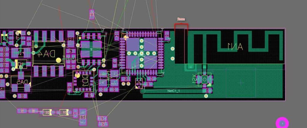
Creating the Board Outline
The first step in designing a PCB is to create the board outline. In Fusion 360, this is done by creating a sketch and then extruding it to the desired thickness. To create a new sketch, go to the “Sketch” menu and select “Create Sketch”. Draw the outline of the board using the available tools, such as lines, arcs, and circles. Once you have finished the sketch, extrude it to the desired thickness using the “Extrude” tool.
Adding Components
With the board outline created, you can now start adding components to the design. To do this, go to the “Insert” menu and select “Component”. Choose the component you want to add from the available libraries or create a new one. Place the component on the board in the desired location. Repeat this process for all the components you want to add.
Routing the Traces
Once you have added all the components to the board, you can start routing the traces. In Fusion 360, this is done using the “Route” tool. Select the tool and then select the starting and ending points for the trace. Fusion 360 will automatically route the trace between the two points, taking into account any obstacles such as other traces or components. Repeat this process for all the traces you want to route.
That’s it! With these steps, you can create a new PCB design in Fusion 360.
Customizing the PCB Design

Modifying Board Shapes
Fusion 360 allows users to easily modify the shape of their PCB designs. To do this, simply select the “Modify” option in the toolbar and then select the “Board Shape” option. From here, users can add or remove corners, adjust the size of the board, and even add cutouts or slots.
Adding Cutouts and Slots
Adding cutouts and slots to a PCB design is a great way to customize the board for specific applications. In Fusion 360, users can easily add these features by selecting the “Modify” option in the toolbar and then selecting the “Board Shape” option. From here, users can add cutouts and slots by drawing them directly onto the board outline.
Customizing Solder Mask
Customizing the solder mask is an important aspect of PCB design. In Fusion 360, users can easily customize the solder mask by selecting the “Manufacture” option in the toolbar and then selecting the “Solder Mask” option. From here, users can adjust the color of the solder mask, as well as the size and shape of the openings.
Customizing Silkscreen
Silkscreen is a great way to add important information to a PCB design, such as part numbers, logos, or other identifying marks. In Fusion 360, users can easily customize the silkscreen by selecting the “Manufacture” option in the toolbar and then selecting the “Silkscreen” option. From here, users can adjust the size, color, and position of the silkscreen elements.
By customizing the PCB design in these ways, users can create unique and functional boards that meet their specific needs.
Generating Manufacturing Files
When you have finished designing your PCB in Fusion 360, it’s time to generate the manufacturing files. This section will cover how to create Gerber files, generate NC drill files, and export a bill of materials.
Creating Gerber Files
Gerber files are a standard format used by PCB manufacturers to create the copper layers, soldermask, and silkscreen for your PCB. To create Gerber files in Fusion 360, follow these steps:
- Open the PCB design in Fusion 360.
- Click on the “Manufacture” tab at the top of the screen.
- Click on “CAM” in the left-hand menu.
- Select “Gerber” from the list of available CAM operations.
- Choose the layers you want to include in the Gerber files.
- Click “OK” to generate the Gerber files.
Generating NC Drill Files
NC drill files are used by PCB manufacturers to drill the holes in your PCB. To generate NC drill files in Fusion 360, follow these steps:
- Open the PCB design in Fusion 360.
- Click on the “Manufacture” tab at the top of the screen.
- Click on “CAM” in the left-hand menu.
- Select “Drill” from the list of available CAM operations.
- Choose the drill sizes you want to include in the NC drill files.
- Click “OK” to generate the NC drill files.
Exporting Bill of Materials
The bill of materials (BOM) lists all the components used in your PCB design, along with their quantities and reference designators. To export a BOM in Fusion 360, follow these steps:
- Open the PCB design in Fusion 360.
- Click on the “Manufacture” tab at the top of the screen.
- Click on “BOM” in the left-hand menu.
- Choose the format you want to export the BOM in.
- Click “OK” to export the BOM.
In conclusion, generating manufacturing files is an essential step in the PCB design process. By following the steps outlined in this section, you can create Gerber files, NC drill files, and a bill of materials in Fusion 360, making it easy to send your design off to a manufacturer for production.
Collaborating and Sharing Designs
Working with Team Members
Collaborating with team members is a crucial aspect of PCB design, and Fusion 360 makes it easy to work with other designers. You can invite team members to join your project and share designs with them in real-time. This helps to streamline the design process and ensures that everyone is working with the latest version of the design.
Fusion 360 also includes version control, so you can easily track changes made by each team member. This helps to prevent conflicts and ensures that everyone is on the same page. Additionally, you can use comments and annotations to communicate with team members and provide feedback on designs.
Sharing Designs with Manufacturing Partners
Once your design is complete, you’ll need to share it with your manufacturing partner. Fusion 360 makes this process easy by allowing you to export your design files in a variety of formats, including Gerber and ODB++. You can also include fabrication notes and other instructions to ensure that your design is manufactured correctly.
Fusion 360 also includes a built-in Design for Manufacturability (DFM) tool that checks your design for manufacturability issues. This helps to ensure that your design can be manufactured efficiently and without errors. You can also use the DFM tool to optimize your design for cost and performance.
In conclusion, Fusion 360 is an excellent tool for collaborating and sharing PCB designs with team members and manufacturing partners. Its intuitive interface, real-time collaboration features, and built-in DFM tool make it easy to work with others and ensure that your design is manufactured correctly.
Conclusion

In conclusion, designing PCBs in Fusion 360 is a powerful and efficient way to create custom circuit boards for your projects. With its intuitive interface and robust set of tools, you can quickly and easily create complex designs that meet your specific requirements.
One of the key benefits of using Fusion 360 for PCB design is the integration with other design and engineering tools. This allows you to seamlessly move from concept to production, without the need for multiple software programs or file conversions.
Another advantage of Fusion 360 is the ability to collaborate with others on your PCB designs. You can share your designs with team members, suppliers, and manufacturers, and work together in real-time to make changes and improvements.
Overall, Fusion 360 is a powerful and versatile tool for PCB design that can help you bring your ideas to life. Whether you’re a professional engineer or a hobbyist, this software can help you create high-quality, custom circuit boards that meet your unique needs and specifications.
