Printed Circuit Boards (PCBs) are a crucial component of modern electronics, found in a wide range of devices from smartphones to complex laboratory equipment. PCB manufacturing involves multiple processes to create precise and reliable boards, ensuring seamless functionality in electronic devices. With the increasing intricacy of electronic devices, understanding the basics of PCB fabrication is essential to streamline production, reduce costs, and enhance device performance.
The PCB fabrication process involves six major steps: design, material selection, patterning, etching, drilling, and assembly. Design is a crucial step in which engineers lay out the circuit’s components and create a blueprint for the board. Material selection, generally consisting of copper-clad laminate and glass-reinforced epoxy, ensures the correct properties for functionality and durability of the board. Patterning, etching, and drilling involve shaping and creating the pathways for electrical connections.
Knowing the intricacies of PCB fabrication helps electronic manufacturers make informed decisions that result in better quality and more efficient products. Adopting advanced manufacturing techniques like multilayer or flexible boards can significantly improve a product’s performance and longevity. Familiarity with the fabrication process allows manufacturers to not only create better products but also minimize errors, streamline production, and ultimately remain competitive in today’s technology-driven world.
Basics of PCB Fabrication
Creating the Schematic
A printed circuit board (PCB) fabrication starts with creating a schematic, a blueprint for the electronic circuit. This step involves determining the essential components and their connections to achieve the desired functionality. Designers use schematic capture software to convert the abstract representation of the electronic circuit into a detailed, organized diagram. Once finished, a thorough review and verification of the schematic ensure that it meets the design requirements.
Board Design
The next step in PCB fabrication is board design. The designed schematic is imported into a PCB layout CAD (Computer-Aided Design) tool. This software enables you to arrange the components on the board and route the interconnecting traces between them. Considerations in this stage include trace width, spacing, and routing path to ensure optimal signal integrity. Additionally, factors like power distribution, heat dissipation, and mechanical constraints impact board layout decisions.
Proper board design is crucial in achieving reliable and efficient PCB functionality. To aid in this process, many layout tools utilize design rule checks (DRC) and signal integrity analysis to identify and correct potential issues. Once the board design is complete, the final step is to generate manufacturing files like Gerber files and drill files. These files serve as instructions guiding the PCB production process.
PCB Materials
Printed Circuit Boards (PCBs) are made up of various materials that provide the necessary structure, electrical conductivity, and insulation. Choosing the right materials can significantly impact the performance and reliability of the final product. Some key materials used in PCB fabrication include:
-
Substrate: The most common substrate is FR-4, a glass fiber epoxy laminate, known for its outstanding mechanical and electrical properties. Other materials, like aluminum or polyimide, can be used for special application requirements.
-
Copper: Copper is often used for conducting layers, due to its excellent electrical conductivity and heat dissipation properties. The copper thickness can vary depending on the specific design and power requirements.
-
Solder Mask: A solder mask, typically made of epoxy or liquid photo-imageable (LPI) material, is applied to the PCB to prevent bridging and oxidation. The mask also helps protect the copper traces from moisture, chemicals, and physical damage.
-
Silkscreen: Silkscreen layers, usually made of epoxy ink or LPI, are applied to provide identification marks, such as component labels, reference designators, and logos.
Each PCB material has its advantages and disadvantages when it comes to specific factors like cost, performance, and manufacturing complexity. For instance:
| Material | Pros | Cons |
|---|---|---|
| FR-4 | Cost-effective, widely available | Limited thermal performance |
| Aluminum | Excellent thermal conduction, durability | Higher cost, limited flexibility |
| Polyimide | High flexibility for flex PCBs, heat resistance | Expensive, complex manufacturing process |
Knowing the properties of each material and their suitability for a specific application is crucial for designers and manufacturers to create reliable, high-performing PCBs.
PCB Fabrication Process

Lamination
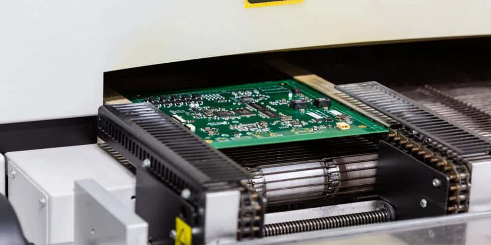
The lamination process is essential in creating a reliable PCB. It involves applying heat and pressure to bond multiple layers of copper and insulating material (prepreg) together. The result is a multilayer PCB with excellent electrical and structural properties.
Drilling
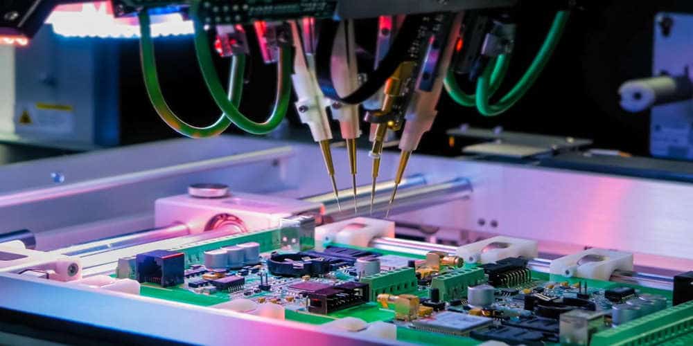
Drilling is the next step in the PCB fabrication process. It involves creating holes in the PCB to accommodate various components such as vias and through-hole components. Drill sizes are typically chosen based on the specific requirements of the design. Precision machinery, such as CNC machines, are used to ensure accurate drilling of the holes.
Etching
Etching is a critical part of the PCB fabrication process as it removes unwanted copper from the board to create the desired circuit patterns. The most common method is to use chemical solutions, such as ferric chloride or ammonium persulfate, to dissolve the unwanted copper. The areas that need to remain protected are typically covered with a photoresist, which resists the etching chemicals.
Solder Mask
The solder mask is an integral layer applied to the PCB to protect the copper traces and to prevent solder bridges between closely spaced traces or pads during soldering. The solder mask is typically a green epoxy material, but other colors can be used depending on the project’s aesthetic requirements. The solder mask is applied using a screen-printing process or photo-imaging methods.
Silkscreen Printing
Silkscreen printing is the final step in the PCB fabrication process, and it’s used to label reference designators, component symbols, logos, and other essential information on the board. The silkscreen color usually contrasts the solder mask to ensure visibility. The most common ink colors are white, black, or yellow, and the process can be done using screen-printing or inkjet printing methods.
PCB Manufacturing Methods
Subtractive Method
The subtractive method is the most commonly used technique in PCB fabrication. It involves removing unwanted copper material from the board to create the desired circuit pattern. The process typically starts with a copper-clad laminate, followed by a photoresist layer that is exposed to UV light using a photomask with the desired circuit design. The exposed areas will harden, while the unexposed areas are removed using a chemical etching solution. Finally, the hardened photoresist is stripped off, leaving only the desired copper traces on the PCB.
Some key advantages of the subtractive method include:
- Well-established process with readily available materials and equipment
- Suitable for a wide range of applications, from simple to high-density designs
- Relatively low production costs
Additive Method
In contrast to the subtractive method, the additive method deposits copper directly onto the desired areas of the PCB. This process begins with a substrate coated with a thin layer of copper. A photoresist is then applied, and a photomask is used to expose the desired circuit pattern to UV light. The exposed areas harden, and an electroplating process is used to deposit additional copper onto these areas. The unexposed photoresist is then removed, along with the underlying thin copper layer, revealing the desired circuit pattern.
Some of the advantages of the additive method include:
- Less copper waste, making it an environmentally friendly option
- More precise and finer line definition, suitable for high-density designs
- Greater design flexibility
Both subtractive and additive methods have their own merits, and the choice between them depends on factors such as design complexity, production volume, and cost considerations. Each method has proved effective in producing high-quality PCBs in various applications.
Quality Control in PCB Fabrication
Quality control plays a crucial role in PCB fabrication to ensure that the final product meets the desired specifications and functions reliably. Several measures are put in place to maintain high standards throughout the process.
Inspection Methods
Various inspection methods are employed at different stages of PCB fabrication. These include:
-
Automated Optical Inspection (AOI): This technique uses cameras and image-processing software to quickly and accurately identify defects or deviations from the design.
-
X-ray Inspection: It allows the inspection of hidden features, such as the quality of solder joints and the alignment of buried components.
Test Procedures
Once the PCBs are assembled, they must be tested for functionality and performance. Common test procedures include:
-
In-circuit Test (ICT): An ICT fixture checks for component values, presence, polarity, and basic functionality by applying electrical signals to the assembled board, measuring its response, and comparing the results to the expected values.
-
Functional Test (FCT): This test simulates the real-world operating conditions of the PCB to ensure that it performs as designed under all conditions.
Material and Component Selection
Ensuring high-quality PCB fabrication starts with choosing the right materials and components. Some key factors to consider include:
-
Substrate material: The choice of substrate (such as FR-4, polyimide or others) influences the board’s mechanical, electrical, and thermal properties.
-
Copper thickness: The thickness of the copper layer impacts the current-carrying capacity and signal integrity of the PCB.
-
Component quality: Selecting reputable manufacturers and suppliers helps ensure that the components used are reliable and meet the required specifications.
Following these quality control measures in PCB fabrication minimizes the risk of defects and ensures that the final product is reliable, durable, and performs as expected.
The Role of Design For Manufacturability (DFM)
Design for Manufacturability (DFM) is a critical aspect of the PCB fabrication process. The primary goal of DFM is to ensure that the PCB design can be efficiently and reliably manufactured at the desired scale, while maintaining quality and performance.
One key element of effective DFM is the selection of appropriate materials and substrate to match the intended performance of the device. Material selection is determined by factors such as:
- Thermal properties
- Mechanical strength
- Electrical performance
Another aspect of DFM is optimizing the layout of components and traces within the board. This can include:
- Minimizing trace length to reduce signal propagation delays
- Balanced copper distribution to prevent warping
- Adequate spacing between components to avoid short-circuiting
To achieve a successful DFM process, designers should also consider the manufacturing constraints of their chosen fabricator. Different fabricators may have varying tolerances and capabilities, which can impact the final product. Some factors to take into account include:
- Drill hole size and accuracy
- Minimum trace width and spacing
- Supported surface finishes
Lastly, it is important to thoroughly verify the design before submitting it for fabrication. This can be done through rigorous design rule checks (DRC), which help identify potential issues and ensure the design meets all manufacturing requirements. By addressing these concerns early in the process, designers can minimize the need for costly and time-consuming design revisions.
Types of PCB Fabrication Services
PCB fabrication services are crucial for creating custom printed circuit boards tailored to specific project requirements. There are several types of services available, each with their own advantages and disadvantages.
Single-Sided PCBs
Single-sided PCBs are the most basic type of printed circuit board. They have one layer of conductive material, typically copper, placed on one side of the insulating substrate. This type of PCB is useful for simple applications and is generally less expensive than other options.
Double-Sided PCBs
Double-sided PCBs have conductive material on both sides of the substrate. With this type, components can be mounted on both sides, allowing for more complex circuitry. Double-sided PCBs require additional fabrication steps, such as plated through holes (PTH) to connect the two layers of copper, making them more expensive than single-sided PCBs.
Multi-Layer PCBs
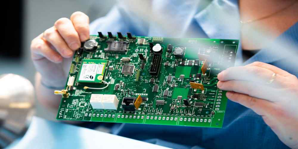
Multi-layer PCBs consist of multiple layers of conductive material separated by insulating material. These PCBs allow for higher component density and are suitable for more advanced applications within industries like aerospace and telecommunications. Multi-layer PCBs can range from four to over 30 layers, with each additional layer increasing the cost and complexity of the fabrication process.
Flex PCBs
Flex PCBs use a flexible material, such as polyimide, as the insulating substrate. This type of PCB offers design flexibility, allowing for bending and folding, making it ideal for compact or unconventional designs. Flex PCBs have a higher cost compared to rigid options, but the benefits can outweigh these costs in certain applications.
Rigid-Flex PCBs
Rigid-flex PCBs combine the features of both flex and rigid PCBs. This type of fabrication service entails creating a multi-layer PCB with both rigid and flexible sections. Rigid-flex PCBs are typically used in applications requiring high-density circuits and mechanical strength.
Each type of PCB fabrication service offers unique benefits and is suitable for specific applications. The choice between these services depends on factors such as design complexity, space constraints, and budget.
Choosing a PCB Fabrication Manufacturer
When selecting a PCB fabrication manufacturer, it is crucial to consider several factors to ensure high-quality results and a smooth process. To make an informed decision, assess the following elements:
-
Experience: Choose a manufacturer with extensive experience in producing different types of PCBs. It is helpful to select a company that works with various industries, as it indicates their adaptability to different requirements.
-
Certifications and Quality Standards: Verify the manufacturer’s certifications, such as ISO 9001 and UL approval. These certifications demonstrate the company’s commitment to quality and industry standards.
-
Production Capacity: Assess the manufacturer’s production capacity to ensure they can meet your project’s volume and timeline requirements. It is advisable to choose a company with multiple production lines to minimize potential delays.
-
Technical Capabilities: Confirm that the manufacturer can accommodate your project’s specific design requirements, such as board thickness, layer count, and surface finish. Verify their technological capabilities to address unique or complex requirements.
-
Customer Support and Communication: Effective communication is vital for a successful project. Choose a manufacturer with a dedicated customer support team and open channels for addressing questions, concerns, or changes in your project. It is also crucial for the manufacturer to provide design for manufacturability (DFM) feedback during the quoting process.
Keep these factors in mind while choosing a PCB fabrication manufacturer, as they can significantly impact the final outcome and satisfaction of your project.
Conclusion
PCB fabrication is a crucial step in the electronics manufacturing process. Understanding the various aspects involved can help ensure a high-quality end result. By selecting appropriate materials, design software, and manufacturing techniques, a well-functioning PCB can be produced.
Several key factors to consider include the choice of substrate material and copper weight. These decisions can greatly impact the overall performance and lifespan of the board. Additionally, working with reliable PCB fabrication partners is essential for meeting industry standards and avoiding costly mistakes.
In summary, a comprehensive understanding of the PCB fabrication process can lead to more efficient and robust electronic devices. With careful attention to detail and adherence to best practices, successful outcomes are more likely to be achieved.
