In recent years, the demand for sophisticated electronics has surged, making printed circuit board (PCB) layout design more critical than ever. PCB layout design service plays a pivotal role in electronics design, as it provides the framework for connecting components and creating efficient circuits. As technology advances, PCB designers face increased challenges in designing complex, high-density boards that meet industry standards and competition demands.
A proficient PCB layout design service is essential for ensuring the seamless functionality and reliability of electronic circuits. Specialists in this field possess the expertise to optimize stack-up configuration, component routing, and ground-plane management. A well-designed PCB layout not only minimizes electromagnetic interference (EMI) but also reduces the overall footprint and manufacturing costs.
The rapidly developing world of electronics relies heavily on PCB layout design services that provide innovative solutions tailored to clients’ specific needs. Skilful designers consider factors like signal integrity, thermal performance, manufacturability, and compliance with regulations to deliver high-quality products. Staying up-to-date with industry trends and technological advancements maximizes a design’s performance, longevity, and market competitiveness.
PCB Layout Design Service Overview
Role in Electronics Industry
Printed Circuit Board (PCB) layout design services play a crucial role in the electronics industry. PCB designers work on creating efficient and reliable circuit boards for various electronic devices and systems. From smartphones and medical equipment to aerospace and automotive applications, PCB layouts underpin the functionality of countless products.
Types of Services Offered
PCB layout design services typically offer a range of solutions to cater to diverse industry needs:
- Single-layer PCBs: These simple designs contain a single layer of conductive material, typically copper, on one side of the board. They are suitable for basic electronic devices.
- Double-layer PCBs: Featuring conductive layers on both sides, these boards allow for increased complexity and higher density components.
- Multilayer PCBs: Ideal for high-performance devices, these boards stack multiple conductive layers, separated by insulating material. They enable high-speed signal routing and a compact design.
- Flexible and Rigid-flex PCBs: Made from flexible materials, these boards can bend and twist to fit specific requirements, offering increased durability and versatile applications.
In addition, PCB layout design services may provide auxiliary services such as schematic design, component selection, and signal integrity analysis.
Key Stages of PCB Layout Design Process
Design Requirements
The design requirements stage involves defining the specific characteristics and functionalities of the PCB. This can include electrical requirements, dimensions, and material specifications. By establishing this foundation, designers can ensure that the end-product will meet the necessary requirements.
Schematic Design
Schematic design involves creating a visual representation of the circuit connections and components. This representation serves as a blueprint for the layout stage. During this phase, the designer ensures that there is a logical flow of signals and power between components.
Component Placement
During the component placement stage, the components are strategically placed on the PCB. This involves consideration of many factors, including signal integrity, power distribution, thermal management, and mechanical constraints. Ensuring proper placement can have a significant impact on the overall performance and reliability of the design.
Routing and Grounding
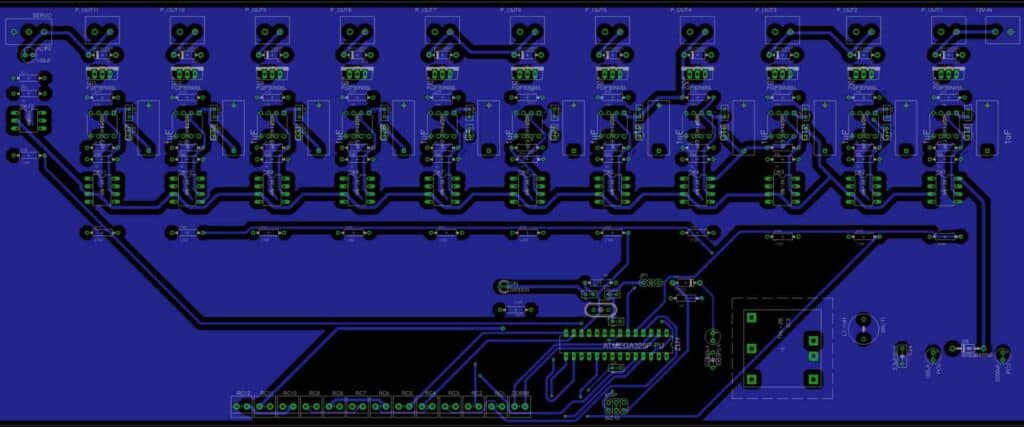
In the routing phase, the designer determines the best path for signal traces between components while avoiding interference and minimizing signal degradation. Grounding is critical for minimizing noise and maintaining signal integrity. Proper routing and grounding techniques help ensure optimal performance and reduce the likelihood of errors or failures.
Gerber File Generation
Gerber files provide detailed manufacturing specifications for the PCB’s various layers, including copper traces, solder mask, and silkscreen. These files are critical in the PCB fabrication process, allowing manufacturers to accurately produce the designed board. Generating accurate Gerber files is essential for ensuring a successful production run.
Essential PCB Layout Design Principles

Signal Integrity
Signal integrity is a critical aspect of PCB layout design. It refers to the quality of the electrical signals transmitted through the PCB. To maintain signal integrity, designers need to consider factors such as trace geometry, impedance, signal crosstalk, and grounding. Effective techniques include minimizing trace lengths, using differential signaling, and utilizing ground and power planes.
Power Distribution Network
A robust power distribution network (PDN) is essential for stable and efficient PCB operation. Designers must ensure that all components receive a stable and noise-free power supply. They should consider the following in PDN design:
- Proper placement of decoupling capacitors for noise reduction
- Minimizing current loop areas to reduce inductance
- Using proper trace widths and thicknesses for power delivery
- Implementing separate planes for digital and analog power supplies
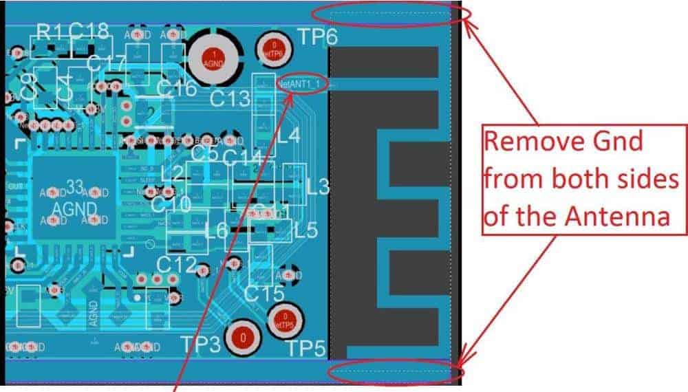
Electromagnetic Compatibility
Electromagnetic compatibility (EMC) involves ensuring that a PCB does not emit or absorb excessive electromagnetic noise. EMC design techniques include:
- Properly grounding PCB components
- Using a multi-layer board with dedicated ground and power planes
- Implementing various trace length matching techniques for high-speed signals
- Incorporating proper shielding for sensitive components
Thermal Management
Managing heat dissipation is crucial for maintaining optimal performance and ensuring component reliability. Key thermal management principles in PCB layout design include:
- Proper component placement to avoid hotspots
- Using heat sinks and thermal vias for high-power components
- Allocating sufficient copper areas for heat dissipation
- Implementing effective airflow strategies in the enclosure
Software Tools for PCB Layout Design
When it comes to PCB layout design, there are several software tools that can help streamline the process and provide the necessary features for creating efficient and high-quality designs. In this section, we will look at some of the most popular and commonly used tools: OrCAD, Altium Designer, EAGLE, and KiCad.
OrCAD
OrCAD is a well-known and widely used PCB layout design software developed by Cadence Design Systems. Some key features of OrCAD include:
- Schematic capture and simulation tools
- Advanced routing capabilities
- Hierarchical design management
- Library and part management
Altium Designer
Altium Designer is another popular choice for PCB layout design, offering a comprehensive set of tools and features. Key aspects of Altium Designer include:
- Intuitive user interface
- 3D visualization and clearance checking
- Flex and rigid-flex design capabilities
- Design rule checks and electrical rule checks
EAGLE
EAGLE, developed by Autodesk, is a user-friendly PCB layout design software with a strong community of users. Some significant features of EAGLE include:
- Access to a vast component library
- Easy to learn and use
- Affordable pricing
- Strong integration with Fusion 360
KiCad
KiCad is an open-source PCB layout design software that has been gaining popularity due to its features and being free of cost. Key features of KiCad include:
- Cross-platform compatibility
- Advanced design rule checks
- Customizable component libraries
- Intuitive user interface
Quality Assurance and Testing
Design Rule Check
Design Rule Check (DRC) is a critical step in the PCB layout design process, ensuring that the layout follows the guidelines set by the fabrication house. It helps detect errors before the manufacturing process, reducing the risk of costly rework.
- Validate trace widths and spacing
- Check for minimum drill sizes
- Confirm component clearances
To confirm that the design adheres to the required specs, PCB designers utilize DRC tools within their CAD software to detect any rule violations and correct them promptly.
Design for Manufacturability
Another essential aspect of quality assurance in PCB layout design is Design for Manufacturability (DFM). It focuses on designing PCBs to ensure a smooth manufacturing process. The primary goal of DFM is to reduce costs, enhance quality, and minimize the need for any modifications during production. Some considerations for DFM include:
- Properly sized solder pads
- Adequate trace widths for current handling
- Optimal component placement
- Considering the available fabrication technologies
Implementing quality assurance and testing processes like Design Rule Check and Design for Manufacturability in PCB layout design services is vital for successful board production and meeting the overall project requirements.
Choosing a PCB Layout Design Service
Experience and Expertise
When selecting a PCB layout design service, it’s crucial to consider the experience and expertise of the team. A company with a proven record of successful PCB designs and satisfied clients will ensure that your project is in good hands. Look for a portfolio showcasing their previous work, as well as certifications and industry affiliations.
Flexibility and Scalability
A good PCB layout design service should offer flexibility and scalability to adjust to your project’s requirements. Whether you need a simple design for a prototype, or a complex multi-layered board for a production run, the service should be able to accommodate your needs. Consider the following aspects:
- Types of PCBs they can design (rigid, flexible, etc.)
- Ability to work with various software and design tools
- Capacity to handle different production volumes
Communication and Support
Transparent communication and reliable support are essential components of a satisfactory PCB layout design service experience. Ensure that the company you select offers:
- Clear communication channels (email, phone, etc.)
- Timely responses to questions and requests
- Willingness to collaborate and implement design changes
- Post-design support, such as documentation and quality assurance checks
Considering these factors will help you make an informed decision when choosing a PCB layout design service.
Industry Trends and Future Outlook
The PCB layout design service industry is seeing significant growth, driven by increasing demand for smart devices, automotive electronics, and innovative technologies. As consumer demands evolve, electronic devices are getting smaller, more intricate, and more powerful, putting pressure on the PCB design process to provide faster, more efficient, and reliable designs.
An emerging industry trend is the automation of the PCB layout design process. This involves the use of advanced algorithms and sophisticated design software to reduce human error and improve efficiency. Particularly, artificial intelligence (AI) and machine learning (ML) technologies are being incorporated into these tools to make smarter design decisions.
- Automation and AI/ML: PCB design software providers are placing a strong emphasis on developing increasingly sophisticated automation features, integrating AI and ML technologies to assist designers in creating more accurate and efficient PCB layouts.
- Cloud-based PCB design tools: As collaboration becomes more important in the design process, cloud-based PCB design tools offer the ability to work remotely and share projects in real-time, streamlining the development process and reducing development time.
- Modular design: As device size continues shrinking, modular design techniques are growing in importance. These allow multiple circuit components to be integrated into a single module, improving device performance and reducing the need for complex wiring and cabling.
- Advanced materials: The development of new materials with improved characteristics, such as high-temperature resistance and better electrical performance, is expanding the possibilities for PCB design.
The future outlook for the PCB layout design service industry is promising, with a continued emphasis on technology advancements, improving collaboration, and expanding the use of advanced materials. As a result, the PCB design process is expected to become increasingly efficient, accurate, and adaptable to the fast-paced demands of the modern world.
