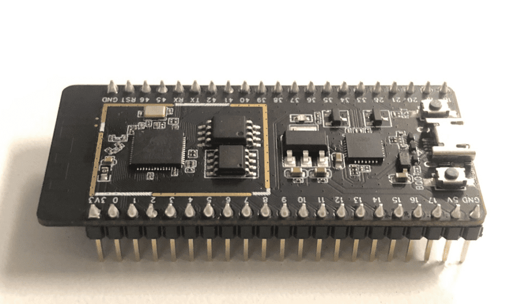
The ESP32 WROOM module is a popular choice for Internet of Things (IoT) projects due to its low power consumption, Bluetooth and Wi-Fi connectivity, and affordable price. However, designing a printed circuit board (PCB) layout for the ESP32 WROOM module can be a challenging task, especially for beginners.
In this article, we will provide an overview of the ESP32 WROOM PCB layout and discuss some best practices for designing a PCB layout for this module. We will cover topics such as component placement, trace routing, power supply design, and grounding techniques. Whether you are a hobbyist or a professional engineer, this article will provide you with valuable insights into designing a robust and reliable PCB layout for your ESP32 WROOM project.
ESP32-WROOM PCB Layout Basics
Schematic Design
The first step in designing a PCB layout for ESP32-WROOM is to create a schematic design. The schematic design should include all the necessary components and their connections. It is essential to follow the datasheet’s recommended schematic design to ensure the proper functioning of the module.
PCB Layout Guidelines
After creating the schematic design, the next step is to create the PCB layout. Here are some guidelines to follow when designing the PCB layout for ESP32-WROOM:
-
Keep the power supply traces short: The power supply traces should be kept short to minimize the voltage drop and noise. It is recommended to use a four-layer PCB with a separate power plane.
-
Place decoupling capacitors close to the power pins: Decoupling capacitors should be placed as close as possible to the power pins to reduce the noise and voltage fluctuations.
-
Separate the analog and digital ground planes: The analog and digital ground planes should be separated to avoid the noise from the digital circuits affecting the analog circuits.
-
Keep the RF traces short and direct: The RF traces should be kept short and direct to minimize the loss and noise. It is recommended to use a 50-ohm impedance trace for RF signals.
-
Use proper clearance and trace width: The clearance and trace width should be selected based on the current-carrying capacity and voltage requirements of the circuit.
-
Avoid sharp corners and right angles: Sharp corners and right angles should be avoided as they can cause signal reflections and noise.
-
Follow the recommended placement and orientation of components: The placement and orientation of components should follow the recommended guidelines in the datasheet.
By following these guidelines, you can design a reliable and efficient PCB layout for ESP32-WROOM.
Power and Ground Planes

Power Plane Design
The power plane is an essential part of the PCB layout for the ESP32 WROOM module. It provides a low impedance path for the power supply to reach all the components on the board. The power plane should be designed to have a solid, uninterrupted ground plane, which provides a return path for the current. A good power plane design can help reduce noise and improve the performance of the circuit.
When designing the power plane, it is important to consider the power requirements of the ESP32 WROOM module and any other components on the board. The power plane should be designed to handle the maximum current requirements of the module and other components. The thickness of the copper layer should be chosen accordingly.
Ground Plane Design
The ground plane is an essential part of the PCB layout for the ESP32 WROOM module. It provides a low impedance path for the return current to flow. The ground plane should be designed to have a solid, uninterrupted connection to the power plane. A good ground plane design can help reduce noise and improve the performance of the circuit.
When designing the ground plane, it is important to consider the ground requirements of the ESP32 WROOM module and any other components on the board. The ground plane should be designed to handle the maximum current requirements of the module and other components. The thickness of the copper layer should be chosen accordingly.
In conclusion, a well-designed power and ground plane is essential for the proper functioning of the ESP32 WROOM module. It is important to consider the power and ground requirements of the module and other components on the board when designing the power and ground planes. A good power and ground plane design can help reduce noise and improve the performance of the circuit.
ESP32-WROOM Signal Routing
Signal Integrity Considerations
When laying out the ESP32-WROOM PCB, it is important to consider the signal integrity of the design. To ensure proper signal integrity, the following considerations should be taken into account:
- Keep the signal traces as short as possible
- Use a ground plane to reduce noise and interference
- Use decoupling capacitors to filter out high-frequency noise
- Use differential pairs for high-speed signals
High-Speed Signal Routing
The ESP32-WROOM has several high-speed signals that require careful routing to maintain signal integrity. These signals include:
- SPI
- I2C
- UART
- SDIO
- Ethernet
To ensure proper routing of these signals, the following guidelines should be followed:
- Keep the signal traces as short as possible
- Use differential pairs for high-speed signals
- Avoid crossing high-speed signals with other traces
- Use vias to connect signal layers
Antenna Design
The ESP32-WROOM has an integrated antenna that requires careful design to ensure proper performance. To optimize the antenna design, the following guidelines should be followed:
- Keep the antenna away from other components and traces
- Use a ground plane to reduce noise and interference
- Ensure that the antenna is not blocked by other components
- Use a matching network to optimize antenna performance
In summary, when designing the ESP32-WROOM PCB layout, it is important to consider signal integrity, high-speed signal routing, and antenna design. By following these guidelines, you can ensure that your design meets the requirements for proper performance and reliability.
ESP32-WROOM PCB Layout Best Practices
When designing a PCB layout for the ESP32-WROOM module, there are several best practices to follow. These practices will help ensure that the module functions optimally and reliably.
Component Placement Guidelines
Proper component placement is crucial for the performance of the ESP32-WROOM module. Here are some guidelines to keep in mind:
- Place decoupling capacitors as close to the power pins of the ESP32-WROOM module as possible to reduce noise and improve stability.
- Place the crystal oscillator as close to the ESP32-WROOM module as possible to minimize trace length and reduce noise.
- Place the antenna trace as far away as possible from other traces and components to reduce interference.
Trace Width and Spacing
Trace width and spacing are also important considerations when designing a PCB layout for the ESP32-WROOM module. Here are some guidelines to follow:
- Use a trace width of at least 10 mils for power and ground traces to reduce resistance and improve stability.
- Use a trace width of at least 6 mils for signal traces to reduce resistance and improve signal integrity.
- Use a spacing of at least 6 mils between signal traces to reduce crosstalk and interference.
Via Placement
Via placement is another important consideration when designing a PCB layout for the ESP32-WROOM module. Here are some guidelines to follow:
- Place vias as close to the pads of the ESP32-WROOM module as possible to reduce impedance and improve signal integrity.
- Use vias with a diameter of at least 0.3 mm to reduce resistance and improve stability.
- Use a spacing of at least 10 mils between vias to reduce crosstalk and interference.
Following these best practices will help ensure that your PCB layout for the ESP32-WROOM module is optimized for performance and reliability.
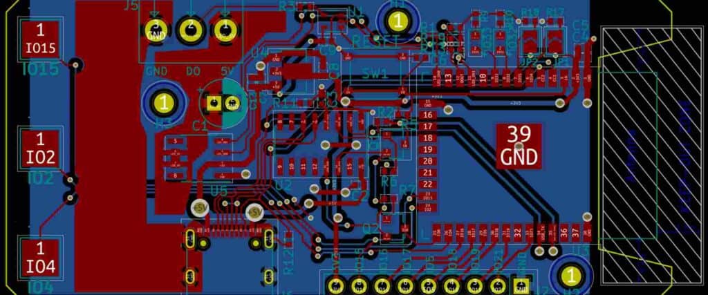
ESP32-WROOM PCB Layout Examples

The ESP32-WROOM module is a powerful and versatile Wi-Fi and Bluetooth module that can be used in a wide range of applications. Proper PCB layout is crucial for the optimal performance of the module. In this section, we will explore some ESP32-WROOM PCB layout examples.
Example 1: Two-Layer PCB Layout
A two-layer PCB layout is the most common and cost-effective option for designing an ESP32-WROOM module. Here are some guidelines to follow when designing a two-layer PCB layout:
- Keep the antenna trace as short as possible and avoid crossing other traces.
- Place decoupling capacitors as close as possible to the ESP32-WROOM module.
- Keep the power supply traces as wide as possible to reduce the voltage drop.
- Avoid placing any components under the ESP32-WROOM module.
Example 2: Four-Layer PCB Layout
A four-layer PCB layout is recommended for high-speed applications or when a high level of noise immunity is required. Here are some guidelines to follow when designing a four-layer PCB layout:
- Use the top and bottom layers for signal routing and the inner layers for power and ground planes.
- Place the decoupling capacitors between the power and ground planes.
- Use a ground plane to reduce noise and improve signal integrity.
- Keep the antenna trace as short as possible and avoid crossing other traces.
Example 3: Six-Layer PCB Layout
A six-layer PCB layout is recommended for applications that require a high level of noise immunity and signal integrity. Here are some guidelines to follow when designing a six-layer PCB layout:
- Use the top and bottom layers for signal routing and the inner layers for power and ground planes.
- Use a separate layer for the antenna trace and keep it away from other traces.
- Place the decoupling capacitors between the power and ground planes.
- Use a ground plane to reduce noise and improve signal integrity.
In conclusion, the ESP32-WROOM module is a powerful and versatile Wi-Fi and Bluetooth module that requires proper PCB layout for optimal performance. By following the guidelines outlined in these examples, you can design a PCB layout that meets your specific requirements.
