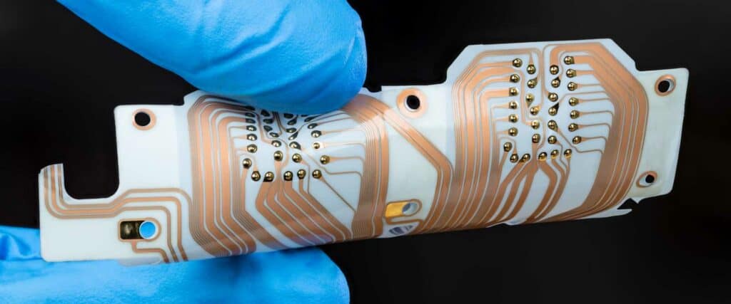
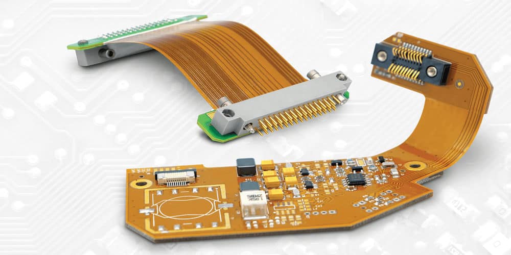
Flexible printed circuit boards (PCBs) are revolutionizing the world of electronics, allowing for more compact and versatile devices. These pliable circuit boards can be bent, twisted, and folded, enabling them to conform to even the most unconventional of shapes and designs.
With the increasing demands for miniaturization and space optimization in modern electronics, flexible PCBs offer a highly desirable solution for both manufacturers and end-users alike. They have become a crucial component in various industries, including aerospace, consumer electronics, and medical devices.
Apart from their flexibility, these circuit boards also offer a range of benefits, such as reduced assembly time, decreased weight, and improved reliability. This makes them an ideal choice for designers looking to push the boundaries of what electronic devices can achieve, leading to a brighter, more connected future.
Flexible PCB: Basics and Benefits
Materials and Construction
Flexible PCBs are typically made from polyimide, a durable and flexible material that helps them withstand mechanical stress. The construction of these boards involves:
- Thin copper layers that act as conductors
- Dielectric materials, such as polyimide, for insulation
- Protective coverlays that provide mechanical and electrical protection
Advantages over Rigid PCBs
There are several benefits to using flexible PCBs compared to rigid counterparts:
- Reduced Weight: Flexible PCBs are lighter because they use thinner and more flexible materials. This helps reduce the overall weight of compact devices.
- Improved Reliability: The use of flexible materials allows the PCBs to bend, providing better resistance against mechanical stress and therefore reducing the likelihood of failure.
- Smaller Devices: Flexible PCBs can be bent and folded into tight spaces, enabling more compact designs.
- Easier Assembly: As these boards can be bent, they’re often easier to work with and install, reducing assembly costs and time.
- Reduced Connection Points: Fewer connections need to be made, as many components can be directly soldered onto the flexible PCB, reducing the number of discrete connections required.
Applications and Industries
Wearable Devices
Flexible PCBs play a vital role in the rapidly growing wearable devices market. These circuit boards provide the ability to conform to the shape of the device and maintain their functionality under various physical stress conditions. Some common wearable devices utilizing flexible PCBs include fitness trackers, smartwatches, and medical monitoring devices.
- Fitness trackers: Flexible PCBs enable compact designs while maintaining device functionality.
- Smartwatches: These devices demand flexibility due to the variety of shapes and sizes on the market, and flexible PCBs help meet these demands.
- Medical monitoring devices: Rely on flexible PCBs for lightweight and compact design, allowing for unobtrusive monitoring.
Automotive
Flexible PCBs have found widespread use in the automotive industry due to their ability to withstand harsh environments and perform well under high temperatures and vibrations. Some examples of automotive applications include:
- LED lighting: Flexible PCBs enable space-saving designs, allowing for innovative lighting solutions in vehicles.
- Engine control modules: These require robust and heat-resistant PCBs, making flexible options ideal.
- Sensors: Flexible PCBs are commonly used in various sensor applications, such as pressure, temperature, and position sensors.
Aerospace
The aerospace industry benefits from the use of flexible PCBs due to their lightweight design and resistance to harsh environmental conditions. Some aerospace applications include:
- Flight control systems: Flexible PCBs help save weight and space in these critical systems.
- Instrumentation panels: These require durable, lightweight, and heat-resistant PCBs, making flexible options suitable.
- Satellite communication systems: Flexible PCBs provide reliable performance under extreme temperature and radiation conditions, critical for satellite communication systems.
Key Design Considerations

Bending Radius and Flexibility
When designing a flexible PCB, it’s crucial to consider the bending radius and flexibility of the materials used. Exceeding the bending radius can lead to increased stress and potential failure. Factors affecting bending radius include:
- Material thickness: Thicker materials generally have a larger bending radius.
- Copper weight: Higher copper weight increases bending radius.
- Component size: Larger components may require a higher bending radius.
It’s essential to keep these factors in mind and select suitable materials and thicknesses when designing a flexible PCB.
Layer Stack-up and Routing
In a flexible PCB, stack-up design and routing play critical roles in ensuring the board functions reliably. A few essential layer stack-up design considerations include:
- Balancing the number of layers: Ensure an even number of layers to prevent warping.
- Staggering traces: Stagger traces to distribute stress more evenly.
- Selecting appropriate dielectric materials: Choosing materials with the right mechanical and electrical properties is vital.
Routing also follows specific guidelines to achieve optimal performance:
- Routing perpendicular to the bend line: This reduces stress build-up in traces.
- Avoiding sharp corners: Eliminate 90-degree angles and use curved bends to minimize stress concentration.
- Employing tear-drop shaped pads: These pad shapes help distribute stress around the pad and trace connections.
Manufacturing Processes and Challenges
Specialized Equipment
Flexible PCBs require specialized equipment when compared to conventional rigid PCBs. Some notable differences in the manufacturing process include:
- Flexible circuits are typically manufactured using roll-to-roll processes, which can be more challenging to control for precision and alignment.
- Lamination processes for flexible materials often require unique adhesives or heat settings to ensure proper bonding of layers.
- Specialized equipment for imaging and etching can be needed to handle the thinner substrates used for flexible circuits.
These differences in equipment can lead to increased costs and complexity in the manufacturing process.
Handling Issues
Handling flexible PCBs during manufacturing can present its own set of challenges:
- Flexible materials are more susceptible to damage, such as tearing or cracking, during handling and processing steps.
- The thin and lightweight nature of flexible circuits makes them more difficult to secure during automated assembly processes.
- Due to their pliability, flexible PCBs may experience misalignment in component placement, leading to defects and increased scrap rates.
Despite these challenges, the demand for flexible PCBs continues to grow, as their benefits of compactness and versatility have proven to be invaluable in modern electronics.
Future Trends and Developments
Flexible PCBs (FPCBs) have become critical in the design and manufacture of compact electronic devices. As demand for sleek, portable technology grows, designers and engineers are seeking innovative solutions to meet the requirements. Here are some future trends and developments for FPCBs:
-
Stretchable FPCBs: The development of stretchable circuit boards is a significant advancement in flexible technology. Instead of just bending, these PCBs will be capable of stretching, offering even greater design versatility in wearables, medical devices, and robotics.
-
Eco-friendly Materials: As environmental concerns become more prevalent, the need for eco-friendly materials in FPCB production will rise. Researchers are exploring alternatives to traditional materials, such as biodegradable polymers and non-toxic adhesives, to minimize the environmental impact.
-
3D Printing: 3D printing technology holds substantial potential in FPCB production. It enables rapid prototyping, customization, and small-batch manufacturing. As advances in 3D printing continue, we can expect to see increased integration of this technology in FPCB fabrication.
-
Embedded Components: Embedding components within the flexible substrate will save space, increase reliability, and enhance performance. As electronics become increasingly compact, the need for integrated, high-density FPCBs will grow.
-
Multilayer FPCBs: As devices become more complex, multilayer FPCBs will need to evolve. Developers are working towards increasing the number of layers while maintaining flexibility and reducing thickness. This advancement will allow for more complex circuitry in a smaller footprint.
These trends and developments will shape the future of FPCB technology, providing innovative solutions to meet the demanding needs of compact electronics. As technology continues to advance, we can expect FPCBs to play an essential role in the evolution of electronic devices.
