Table of Contents
ToggleLayout design is a crucial aspect of electronic circuit design. It involves arranging components on a circuit board in such a way that they function effectively and efficiently. The layout design of an electronic circuit is essential because it determines how well the circuit will perform, how easy it will be to manufacture, and how reliable it will be.
The fundamentals of layout design for electronic circuits include understanding the basic principles of circuit design, knowing the different types of components and their functions, and being familiar with the tools and techniques used in layout design. It is also important to consider factors such as signal integrity, power distribution, and thermal management when designing a circuit layout. By following these fundamentals, designers can create electronic circuits that are optimized for performance, reliability, and manufacturability.

The Importance of Layout Design
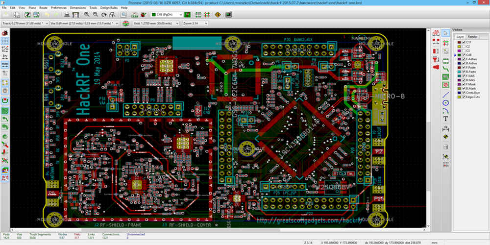
Layout design is a critical aspect of electronic circuit design. It involves the placement of components and routing of traces on a printed circuit board (PCB). A well-designed layout can significantly improve the performance and reliability of a circuit. Here are two important aspects of layout design:
Signal Integrity
Signal integrity refers to the ability of a circuit to maintain the quality of signals as they travel through the PCB. A poor layout can cause signal degradation, resulting in noise, crosstalk, and other issues. To ensure good signal integrity, the following practices should be followed:
- Keep traces as short as possible and minimize the use of vias.
- Maintain a proper distance between traces to prevent crosstalk.
- Use ground planes and power planes to reduce noise and provide a low-impedance path for signals.
- Place decoupling capacitors close to the power pins of components to minimize the effect of noise.
Power Integrity
Power integrity refers to the ability of a circuit to maintain stable and clean power supply voltages. A poor layout can cause voltage drops, ground bounce, and other issues. To ensure good power integrity, the following practices should be followed:
- Use a dedicated power plane for each voltage level to reduce noise and crosstalk.
- Place decoupling capacitors close to the power pins of components to filter out high-frequency noise.
- Use a low-impedance path for power and ground connections to reduce voltage drops and ground bounce.
- Avoid routing high-current traces near sensitive analog or digital circuits to prevent interference.
In conclusion, good layout design is crucial for electronic circuits to function correctly and reliably. By following the best practices for signal integrity and power integrity, you can ensure that your PCB design meets the required specifications and performs optimally.
Design Considerations

When designing electronic circuits, there are several key considerations that must be taken into account to ensure optimal performance. These considerations include component placement, routing, grounding, and decoupling.
Component Placement
Component placement is critical to the overall performance of an electronic circuit. Components must be placed in a way that minimizes the distance between them and optimizes the signal flow. This requires careful consideration of the physical layout of the circuit board, as well as the electrical characteristics of the components themselves.
To optimize component placement, it is important to consider the following:
- The size and shape of the components
- The orientation of the components
- The distance between components
- The proximity of components to signal traces and power planes
- The thermal characteristics of the components
Routing
Routing refers to the process of connecting the various components of an electronic circuit. This involves the design of the signal traces, power planes, and ground planes. The goal of routing is to minimize signal interference and maximize signal integrity.
To optimize routing, it is important to consider the following:
- The length and width of signal traces
- The placement of vias
- The use of differential signaling
- The use of shielding
- The use of impedance matching
Grounding
Grounding is critical to the performance of an electronic circuit. A solid ground connection is necessary to provide a stable reference voltage for the circuit. This helps to minimize noise and interference, and ensures that the circuit operates within its intended parameters.
To optimize grounding, it is important to consider the following:
- The placement of ground planes
- The use of ground vias
- The routing of ground traces
- The use of ground loops
- The use of EMI shielding
Decoupling
Decoupling refers to the use of capacitors to filter out noise and interference in an electronic circuit. Decoupling capacitors are typically placed as close as possible to the power pins of the components they are intended to protect. This helps to ensure that the power supply is stable and that the circuit operates within its intended parameters.
To optimize decoupling, it is important to consider the following:
- The placement of decoupling capacitors
- The value and type of decoupling capacitors
- The routing of the power supply traces
- The use of multiple decoupling capacitors in parallel
Overall, the design considerations outlined above are critical to the performance of any electronic circuit. By carefully considering each of these factors, designers can optimize the layout of their circuits and ensure that they operate reliably and efficiently.
Circuit Simulation

Circuit simulation is a crucial step in electronic circuit design. It allows designers to test and verify their circuits before they are physically built. This saves time and money by catching errors early in the design process. There are two main types of circuit simulation: analog and digital.
Types of Simulation
Analog Simulation
Analog simulation is used to model circuits that operate on continuous signals. This includes circuits that use voltage and current to represent signals, such as amplifiers and filters. Analog simulation tools use mathematical models to predict how a circuit will behave under different conditions.
Digital Simulation
Digital simulation is used to model circuits that operate on discrete signals. This includes circuits that use binary signals to represent data, such as logic gates and flip-flops. Digital simulation tools use logic models to predict how a circuit will behave under different conditions.
Simulation Tools
There are many simulation tools available for electronic circuit design. Some popular options include:
- SPICE (Simulation Program with Integrated Circuit Emphasis)
- LTSpice
- Multisim
- CircuitMaker
These tools allow designers to create and simulate circuits using a graphical interface. They provide a variety of analysis options, such as AC analysis, transient analysis, and Monte Carlo analysis. Simulation results can be viewed in various formats, such as graphs and tables.
In conclusion, circuit simulation is an essential part of electronic circuit design. It allows designers to catch errors early and save time and money. There are two main types of simulation: analog and digital. Popular simulation tools include SPICE, LTSpice, Multisim, and CircuitMaker.
Design for Manufacturability

Design for Manufacturability (DFM) is an essential aspect of layout design for electronic circuits. DFM is the process of designing a product in a way that makes it easy to manufacture, assemble, and test. DFM is crucial because it helps to reduce the manufacturing cost, improve product quality, and shorten the time-to-market.
One of the critical factors to consider in DFM is the selection of materials. The materials used in the design should be readily available, cost-effective, and easy to work with. The designer should also consider the environmental impact of the materials used in the design.
Another important aspect of DFM is the design of the circuit board itself. The board should be designed in a way that allows for easy assembly and testing. The designer should consider factors such as the placement of components, the routing of traces, and the use of vias.
DFM also involves the use of design rules. Design rules are a set of guidelines that specify the minimum and maximum values for various parameters in the design. These parameters include trace widths, spacing between traces, and the size of vias. By following design rules, the designer can ensure that the design is manufacturable and meets the required specifications.
In conclusion, DFM is a critical aspect of layout design for electronic circuits. By designing for manufacturability, the designer can reduce the manufacturing cost, improve product quality, and shorten the time-to-market. The designer should consider factors such as material selection, board design, and design rules when designing for manufacturability.
Design for Testability
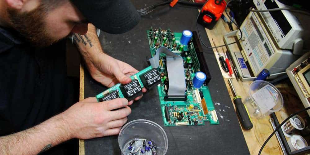
Design for testability is an essential aspect of electronic circuit layout design. It involves designing the circuit in a way that makes it easier to test and diagnose potential issues. By designing for testability, you can save time and money in the long run by avoiding costly repairs and redesigns.
One way to design for testability is to ensure that the circuit has accessible test points. These test points should be strategically placed at key locations in the circuit where potential issues are likely to occur. For example, test points should be placed at the input and output of each stage of the circuit.
Another way to design for testability is to incorporate built-in self-test (BIST) features into the circuit. BIST features allow the circuit to test itself automatically, without the need for external test equipment. This can save time and money, as well as improve the reliability of the circuit.
In addition to test points and BIST features, it is also important to design the circuit with diagnostic capabilities. This can include incorporating error detection and correction features, as well as designing the circuit with fault-tolerant components.
Overall, designing for testability is an important aspect of electronic circuit layout design. By incorporating test points, BIST features, and diagnostic capabilities, you can ensure that your circuit is reliable, easy to test, and easy to diagnose potential issues.
Conclusion

In conclusion, layout design is a crucial aspect of electronic circuit design that must be taken seriously. A well-designed layout can improve circuit performance, reduce noise, and increase reliability. On the other hand, a poorly designed layout can cause signal integrity issues, crosstalk, and other problems that can lead to circuit failure.
To ensure a successful layout design, it is important to follow some fundamental principles. These include understanding the circuit requirements, selecting the appropriate components, optimizing the placement of components, and routing the traces in a way that minimizes noise and signal interference.
Additionally, it is important to pay attention to the physical constraints of the circuit board, such as the size and shape of the board, the location of mounting holes, and the placement of connectors. Using a good CAD tool can help in visualizing and optimizing the layout design.
In summary, a good layout design is a balance between the circuit requirements, the physical constraints of the board, and the design rules of the CAD tool. By following the fundamental principles of layout design, we can create electronic circuits that are reliable, efficient, and perform as intended.

