PCBs or Printed circuit boards are electronic boards which are useful in most electronic devices. These include household appliances, mobile phones, as well as medical equipment.
Typically, the PCBs are also manufactured from the non-substrate materials having copper circuitry layers. Moreover, different PCB types usually differ with respect to their construction. Take for example, though some printed circuit boards have just one copper circuitry layers, the more advanced printed circuit boards (PCBs) may have at least 50
Speaking in general terms, PCB comes in different types. Some popular types include multi layer PCBs, double sided PCBs, and single sided PCBs. To assist you with choosing the best option for your needs, we will be discussing what these PCBs are manufactured from, as well as how they will be able to assist you.
What are the Common Components Found in Printed Circuit Boards?
PCBs are manufactured from different electrical components and PCB materials. Below are the well known PCB components.
Resistors
The resistors help in transmitting electrical current so as to produce a specific voltage as well as dissipate the electric power in the form of heat. Also, they are available in different materials.
Capacitors
Capacitors help in holding an electrical charge inside the board. It then releases it whenever there is a need for more power somewhere else in the circuit. Furthermore, the capacitors function through the collection of opposite charges present on the conductive layers which are separated with the help of a specific insulating material.
Transistors
The transistor serves as an amplifier. It is useful in controlling or switching the electronic signals that are present in circuit boards. Furthermore, there are different transistors available; however, the most common of them all are the bipolar transistors.
Inductors
These function just like the capacitors because they also store energy. Moreover, they are useful in blocking signals inside the printed circuit board like interference coming from a different electronic device.
Diodes
The diode permits the flow of electric current in just one direction. However, it doesn’t flow in the other. Due to this reason, the diodes are useful in stopping the flow of electric current in the wrong direction, as well as causing damage to the board and the entire device. LED or light-emitting diode is the most popular form or type of diode.
Sensors
Sensors are useful in detecting changes occurring in the environmental conditions. It also generates electrical signals which denote the change. Furthermore, the signal is sent to the other components present in the printed circuit board. These sensors help in converting physical elements like air quality, light motion, as well as sound to electrical energy.
What are the Common PCB layers?
All printed circuit boards feature different layers which contribute or add to the functionality. Moreover, no matter the type of PCB you decide to choose, every board has the essential foundation. It means that all the printed circuit boards have these four layers in them.
Copper layer
This layer is manufactured from the copper foil thin layer which is laminated onto the board making use of heat. Referring to the different PCB layers, we mean the number of copper layers present in them.
Take for example, the single sided PCB will feature just one conducting material layers on just one of the board’s sides. For this case, the board’s other side is useful in integrating the different electronic components.
The double sided PCB mounts the components and conductive copper foil on the two sides of the circuit board. Also, the copper layer thickness determines the quantity of power required by the PCB to withstand. Printed circuit boards, which have to handle a higher power level will have a thicker copper level.
Substrate layer
The substrate layer is usually manufactured from fiberglass. This is what ensures the rigidity of the board. Also, epoxies can also be used in the pcb manufacturing process of the substrate layers. However, these lack all the durability that can be offered by the fiberglass.
Solder mask layer
This layer of solder mask is placed on the copper top and it offers the majority of printed circuit boards with its green color. The layer helps in insulating the copper and makes sure that it doesn’t touch the other elements in any way.
Silkscreen layer
This layer is majorly added to serve humans. This deals with the addition of numbers, letters, as well as symbols, to the circuit board. Therefore users will find it easy to comprehend the function of the different LEDs and pins.
What Type of Printed Circuit Boards Exists and What are they Manufactured From?

A printed circuit board is made up of both non-conductive and conductive layers, which are all bonded together. Moreover, the PCB materials useful during the assembly and pcb manufacturing process could differ with respect to the board’s purpose as well as the requirements of the client.
Every printed circuit board features different printed circuit board materials. Having all these in mind let us consider the major types of printed circuit boards in detail. We will also outline the major benefits that they offer.
Single sided Printed Circuit Board (PCB)
The single sided PCBs are those boards having a conducting material later on one of the board’s sides. Furthermore, the board’s other side is used in integrating the electronic components. Also, the single sided PCB is composed of the solder mask, conductive metal layer, and the substrate layer.
As a result of their cost-effective and simple design nature, the single sided PCBs are very common. Though this is a simple pcb manufacturing process, they have the ability to be used in a lot of complex electronic devices like vending machines, printers, and stereo equipment.
Double Sided PCB
The double sided printed circuit boards are also called two-layer boards. They permit more complex circuits and designs.
In contrast to the single sided PCBs, the double sided PCBs have the ability to mount conductive copper on the two sides of the circuit board. This ensures closer routing traces. Also, the components present on both boards are connected either through through-hole or surface-mount technology. This depends on what the product needs.
The normal layers that are used in the single sided PCB like solder mask, silkscreen, copper layer, and substrate are useful for the double-sided printed circuit board. However, they are applied to the two sides of the board rather than just one.
As a result of their flexibility and use, the double sided PCB is well-known and popular. This is due to the fact that they permit more complex circuitry. What this means is that you will be able to make use opf them in very advanced electronic systems like car dashboards and lighting.
Multi layer PCB
The multi layer PCB is manufactured and designed making use of different base material layers. Speaking generally, the multi layer PCBs has three conductive layers or more
These printed circuit boards (PCBs) are also constructed making use of the ‘sandwich model’ which has many double-sided conductive layers. These double layers are all separated by the same number of insulating material. Under very high pressures, all these are laminated and bonded together.
Furthermore, the multi layer PCBs offer better functionality for GPS trackers, medical equipment, and computers, coupled with more complex devices and circuits. For complex scenarios such as this, they are preferable to the double sided printed circuit boards. This is due to the fact that the multi layer PCB permits more complex circuits in the smaller footprint.
Rigid PCB
The rigid PCBs are inflexible and solid. They are manufactured from different layers which are all joined making use of heat and an adhesive. With respect to the requirements, the rigid PCBs could either be multi layer, double sided, or single sided.
Furthermore, they are very cost effective and you can produce them in very large quantities. Also, they are hard-wearing. As a result of this, they are useful for industries and products where it is important for components to stay fixed.
Flexible PCB
The flexible PCBs are also called flex circuits or flex PCBs. They are specially designed for fitting into a product or device. Due to this, the flexible PCBs are usually thin and lightweight. Also, they have this great ability of working well in contoured shapes and small spaces.
Flexible PCBs don’t make use of fiberglass for the board’s substrate layer. This is due to the rigidity of the material. To make sure that the board is both durable and flexible, the flexible PCBs make use of plastics like Kapton for its substrate layer.
Also, the flexible PCBs are well-known because they don’t consume much space like other PCB forms. In addition, they have the ability to withstand harsh temperatures. Also, they work with different connectors and components.
Rigid Flex PCB
The rigid flex PCB is the hybrid form of a PCB. Due to this, it combines both the elements of the rigid circuit boards and the flexible circuit boards. As a result of this, you can fold the rigid flex PCBs or flex it continually. During the pcb manufacturing process, it is very common for boards to be transformed into a curve or flexed shape.
Furthermore, the design of the rigid flex PCBs are in 3D. This allows the flexing or twisting of the board to take the desired shape. Asides from this, the rigid flex PCBs come thinner compared to the other PCB forms. With the adhesive-less laminated and thin layer of copper, the rigid flex circuit boards is a light, thin layer, and small solution.
HDI PCB
The HDI PCB or high density interconnect PCB is a new form or type of PCB. As of today, they are known as the fast-growing technologies present in the PCB world. HDI PCBs feature a higher circuitry density in contrast to the traditional printed circuit boards. In addition, the HDI PCBs feature buried and blind vias, coupled with micro vias that feature a much smaller diameter.
What this means is that designers can place the smaller components near themselves on the circuit board. This results in faster signal transmission as well as less crossing delays or signal loss.
Due to these reasons, the HDI PCBs are usually compact and feature fewer layers compared to the multi layer PCBs. However, even though HDI PCBs lack something with respect to the size, they cover up for it in their quality. As a result of this, they are well-known in the advanced technology systems like game consoles and smartphones.
LED PCB
This is a special PCB designed to serve different lighting applications and modules. During the pcb manufacturing process of the LED PCBs, some LEDs (light emitting diodes) are usually mounted to a printed circuit board. This leads to the formation of the complete circuit. This permits total control of how they behave through different switches.
As a result of this, the LED PCBs are useful in many industries in controlling lighting. They are useful in work lamps, torches, street lighting, and automotive lighting.
Blank PCB
The blank PCB is exactly how it sounds. This circuit board is empty and free from any installed components to create a well-functioning printed circuit board.
At times, the blank PCBs are called copper clad circuit boards. This is because of the visible copper layer. Here, this copper plays a very significant role. It makes sure that the board has an efficient and effective energy flow whenever the components are attached on top of the board during the latter stages.
Though some people have the belief that blank PCBs are produced completely from copper, the belief is inaccurate. To ensure that the blank PCBs stay sturdy and durable, then silicon as well as other materials is useful in the manufacturing process. Also, this makes sure that it is a rust-resistant PCB.
In addition, the blank PCBs form the major base in which the securing of the parts and components take place. This circuit board is very popular with the companies having the available technology to assemble as well as manufacture these printed circuit boards, however needs to begin from a blank canvas
Custom PCB
These printed circuit boards are well suited to meet your needs and projects. This company will deliver a completely bespoke solution that takes the custom PCB form.
The custom PCBs now offer a well-known solution. This case is particularly that whereby the PCB design has to be complex, or if there is a need to balance between fabrication and labor costs.
Furthermore, high quality custom PCBs will offer you greater control over all the aspects of the circuit layout. In addition, the custom PCBs also look much more professional to the investors and industry clients.
What are the Steps in the PCB Manufacturing Process?
Typically, the printed circuit boards are made from copper. With respect to the requirements, the plating of the copper is done to a substrate, which is then carved away so as to expose the board’s design. Because there are many layers, they have to be bonded together to ensure a secure fit.
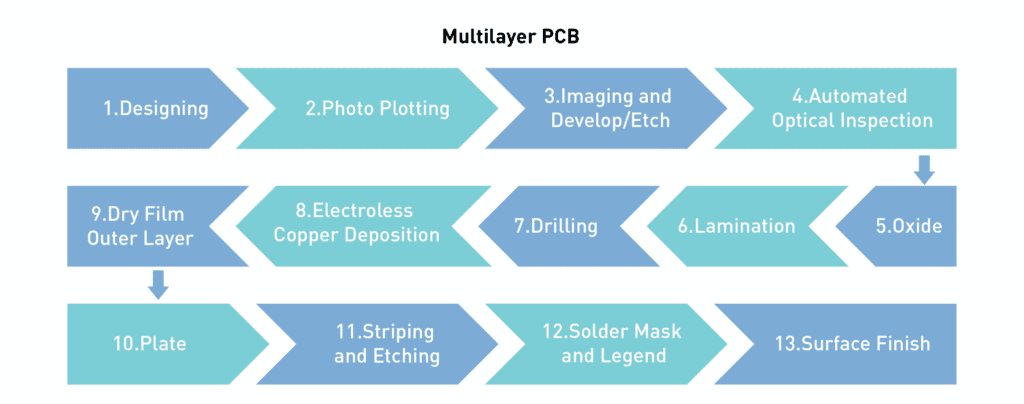
Design
Before the PCB manufacturing process, there’s a need to have the board’s design ready. These blueprints are what you will base the entire process on. This design process is completed via computer software. Making use of the trace width calculator, you will be able to handle most of the details required for the external and internal layers.
Printing of the Design
There’s an important printer known as the plotted printer. This is useful in printing the military PCB design. This creates a film which reveals the board’s layers and details. When it is printed, you will discover two ink colors present on the inner layer of the circuit board.
- Clear ink which shows all the non conductive areas
- Black ink showing the conductive copper circuits and traces
- The outer layers will have the same colors, however, they have a reversed meaning
Creation of the Substrate
At this stage, the PCB starts forming. The substrate which serves as the insulating material (glass fiber and epoxy resin), which holds all the components on its structure, starts forming through the passing of materials via an oven to become semi cured. Furthermore, the pre-bonding of copper is done to the two sides of the layer. Then it is etched away in order to reveal the design from your printed films.
Printing of the Inner Layers
This design is then printed onto a laminate, the structure’s body. The photo-sensitive film, which is manufactured from photo-reactive materials, will harden whenever it becomes exposed to UV light (the resist) helps in covering the structure. This helps in the alignment of the blueprints as well as the board’s actual print. Holes are then drilled into the printed circuit board to assist with the whole alignment process of the inner layers
Ultraviolet Light
Immediately it is aligned, the laminate and the resist will go under ultraviolet lights to help in the hardening of the photoresist. The light goes ahead to reveal the pathways of the copper. Furthermore the blank ink got from earlier, helps in preventing hardening in any areas, which will be removed later. Lastly, the board is washed inside the alkaline solution. This is to get rid of too much photoresist
Getting rid of unwanted copper
This is the time to get rid of unwanted copper still remaining on the board. Here, a chemical solution just like the alkaline solution helps in eating the unwanted copper away. The hardened photoresist stays intact.
Inspection
These layers that are now cleaned will have to undergo inspection for alignment. Those holes that were drilled earlier will assist the alignment of the outer and inner layers. The optical punch machine drills the pin into the holes. This keeps the outer and inner layers all lined up. After this, a second machine then inspects the board. This is to make sure that defects are absent.
Lamination of the layers
Here, you will see that the board is taking shape as these layers are all fused. The metal clamps help in holding the layers altogether as you start the process of lamination. The epoxy resin (prepreg) layer now passes on to the alignment basin. Therefore, a substrate layer then goes over your prepreg, then the copper foil layer, as well as additional prepreg resin. Finally, there is a final copper layer to apply because it is called the press plate.
Pressing of the Layers
A mechanical press is used in pressing all the layers together. The pins are punched all through the layers in order to keep them well secured and aligned. You can remove these pins, but this depends on the technology
If you are doing the right thing, the PCB goes on to your laminating press that applies pressure and heat onto the layers. This epoxy melts the inner part of the prepreg and with pressure, it fuses all the layers together.
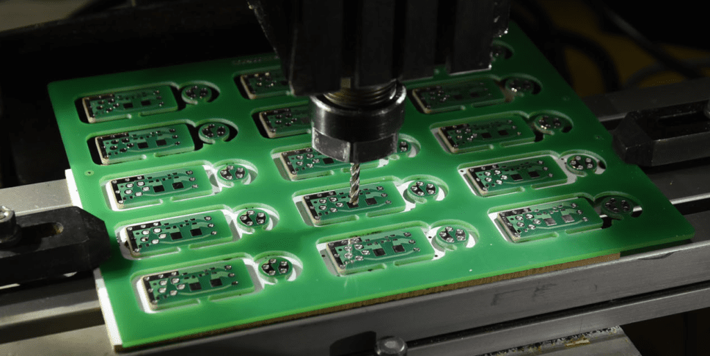
Drilling
Using the computer-guided drill, you then drill holes in the layers. This exposes the inner panels and the substrate. The copper remaining is taken out.
Plating
Now, the board is set to undergo plating. A specific chemical solution helps in fusing the layers together. This board then undergoes thorough cleaning by different chemicals. All these chemicals also help in coating the panel using the thin copper layer that seeps in the drilled holes.
Etching
This same chemical solution gets rid of all unwanted copper found underneath the resist layer. This tin guard layer helps in protecting the required copper.
Solder Mask Application
Before you apply the solder mask ensure you clean all the panels. Next, the solder mask film is used in applying the epoxy. It is this solder mask that applies the usual green color seen on the printed circuit board.
Silkscreening
This process is a very important one since it prints the critical information on the board. Immediately it is applied, the printed circuit board passes through one final curing and coating process.
Surface Finish
The PCB plating is done either with a solderable finish. This depends on your requirements and will increase with respect to the bond and quality of the solder.
Testing
Now before you can say that the PCB is complete, your technician will have to conduct an electrical test on your board. This confirms the functions of the PCB and ensures it follows the initial blueprint designs.
Conclusion
With this article, you should have a good understanding of the PCB manufacturing process or how PCB is made. If you need clarification on any area, please let us know.
