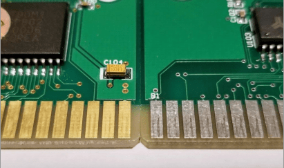
Not only Gold is one of the most electrically conductive materials used for printed circuit boards next to copper and silver but is also highly corrosive-resistant. This paves its way to its application being used as Gold Fingers. It is used as plated narrow connectors between two or multiple adjacent PCBs with Its thickness ranging between 3 to 50 microns.
In today’s advanced technology, separate modules are involved in the process of computing where signals are sent between a number of devices. With the demands of better conductivity where communication of devices is highly observed with signal integrity, gold fingers are utilized in this application.
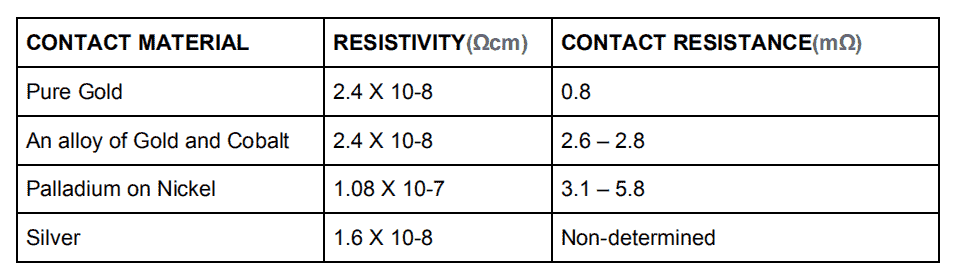
Table 1 : Material
Another criterion that makes Gold suitable for this application is its strength. It is a common practice that Gold Finger PCBs are connected and disconnected several times for maintenance or module replacement purposes. And Gold materials have high strength properties in handling this wear and tear act as it protects the connecting edges. It can be reconnected to different slots up to 1000 times.
1.DESIGN CONSIDERATIONS
As the common designs of Gold Fingers PCB having PIN on both sides, other design considerations are observed below.
- Chamfered Board Edge to certain Angle
These connectors need to be chamfered to around 20 to 45 degrees. The purpose of this is not only for the PCB to be inserted into the socket easily but also to save gold leading to a cheaper board. However, if the board is not intended to be plugged in as often, narrowing is not necessary
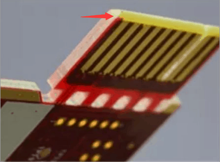
Figure 2. Chamfered Board Edge
- No Laying of Copper on the Gold Finger
Since the gold itself is already a conductor, coating it with copper is not a good practice as it may damage the socket to where it is to be installed and signal integrity can be compromised. This is also one way to prevent exposure at the time of Beveling.
- Inner Layer needs Copper Cutting
The inner layers of the gold finger need to undergo copper cutting. It is the process by which the impedance of the copper under the finger is reduced by cutting it. This is beneficial for the board to avoid ElectroStatic Discharge(ESD).
D. Distance between Gold Fingers and Border Outline
It is a must to follow dimension spacing within PCBs. With any of these are compromised, a malfunction may occur. It is a good practice to have at least a 0.5 mm distance between the gold fingers and the board outline
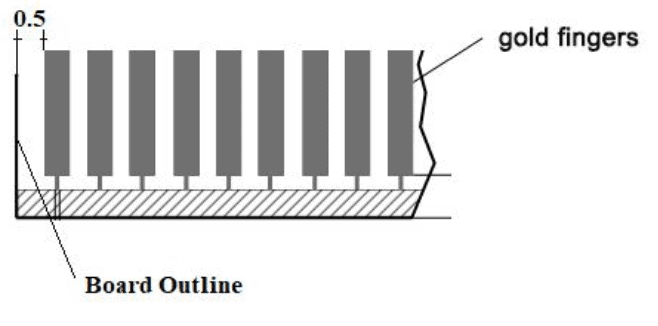
Figure 3. Board Outline Distance
- Gold Finger Location
Gold Finger is placed outward from the PCB’s central location. This is to easily attach and detach the module from any socket.
- Soldermask Restriction
Soldermask and screen printing should not be done within the gold fingers. These restrict the conductivity of the gold fingers once attached to the socket.
G. Plated through holes (PTH) distance
When a-holes are necessary for the PCB, it should not be within the 1 mm distance from the Gold Fingers.
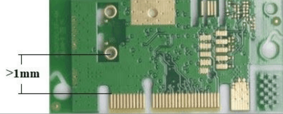
Figure 4. Plated through Holes
These design specifications are highly important for the entire system to communicate with the parent circuit board. consequently , the connecting finger PCB might not fit properly into the appropriate slot.
2.TYPES OF GOLD PLATING
Gold plating has 2 types: Electroless Nickel Immersion Gold and Electroplated Hard Gold. each type differs in properties best suited for commercial and experimental applications.
- Electroless Nickel Immersion Gold(ENIG)
This is a type of gold plating that is more cost-effective. It is easier to solder, soft, and thinner at around 2-5 microinches which makes it least suitable for commercial usage but mostly favorable for experiments and prototypes. It cannot withstand constant plugging and unplug without wearing out.
- Electroplated Hard Gold
This type of gold is more solid and thicker at around 30 microinches. This is mostly applicable to abrasion for commercial purposes. To meet the balance of efficiency and cost-effectiveness, manufacturers use a combination of two types of gold plating techniques.
3. Other Types of Gold Fingers PCB
Since the improvements of PCB designing caters demands of different applications, other types of Gold fingers are utilized. These are unequally sized edge connectors and segmented gold fingers.
- Non-uniform Gold Fingers
Not all gold fingers PCB consists of equal length of conducting connecting edges. For some applications where gold fingers are longer than others, certain links need to be powered up first. One application is a memory card reader
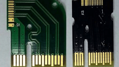
Figure 5. Non-uniform Gold Fingers
- Segmented Gold Fingers
Segmented gold fingers are not only non-uniform in length but also have a disjointed section. This design is made for it to be water-resistant and used for rugged electronic applications were operating well to harsh environments and conditions such as extreme vibration, temperature, and pressure is observed.
Figure 6. Segmented Gold Fingers
4.Manufacturing Gold Fingers PCB
Layering the gold fingers is an essential step in producing this PCB as its thickness requires specification. As its general process, the gold plating is to be applied after the solder mask application.
- Manufacturing Process
Basically, producing this type of PCB involves the preparation of ENIG/hard gold, formation on plating bar, Gold finger Plating, Laser Drilling, Dusting/Cleaning, Sharpening, and electrical testing. Below are the general steps:
Finger pcb gold layer
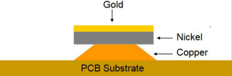
- Nickel Plating
Apply to about three to six microns of nickel to the edge connecting fingers. Its thickness also ranges between 150 and 200 microinches.
- Gold Plating
Add one or two microns of solid gold to the applied edge of the nickel.
- Beveling
Bevel the layer to meet desired height specifications. This is also to easily insert the PCB to the slot. Beveling is typically done at angles of 30 to 45 degrees.
B. Production Standards
A standard in 2012 by Assocation Connecting Electronics Industries(IPC), IPC A-600 and IPC-6010, focuses in PCB Production also concerns Gold Fingers.
- Chemical Composition
About 10 percent of the cobalt composition of gold plating should be used for maximizing rigidity.
- Thickness
A plating thickness of gold fingers should be within 2 to 50 microinches. Standard thicknesses are 0.031, 0.062, 0.093 and 0.0125 microinches. Only for prototyping purposes uses the lesser thicnkesses.
- Visual Testing
The producion of Gold Fingers involves using magnifying lens to inspect smooth edges, clean surface and non-exposure of nickel.
- Tape Test
Once the Gold Finger PCB has been produced, it will undergo tape test where tape is attached to the finger and to observe if gold residue is present on the tape once dettached. Lacks of sufficient adhesiveness happens to PCBs where gold are traced from strip of the tape.
5.Application
The usage of Gold Fingers can be in both commercial and technical where these are utilized in internal circuity.
- Technical Applications
Two main technical applications of gold fingers PCBs are Power Supply and Signal transfer.
- Power Supply Module Connectivity.
Gold Fingers are used to connect a module PCB to a power source from a connecting profile of another larger PCB.
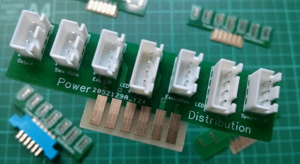
gold finger Power Distribution
- Signal Transfer
Since the primary application of gold fingers is data transfer, signal integrity is maximized when peripheral PCB is connected to a larger board.
Gold finger Signal Transfer
- Commercial Application
In industrial applications, gold fingers are well known, especially when used as connecting devices.
- Video Processing and Connecting Devices
Gold fingers are also specialized to relieve mainboards for video processing and computation
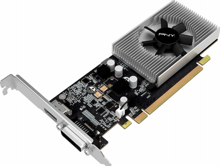
Gold finger Video Processing
- Main Board Processing
Since Gold Fingers are flexible, multiple modules are able to be interconnected within the same board.
Gold finger for mainboard
Gold Finger PCBs contribute to modern advancements in industries to be more productive and more capable which makes technology much more reliable on them. It also has its advantage of upgrading the same system since PCBs are interconnected as long as the connecting contacts are universal which makes the entire system be flexible. By following design specification, standards and choosing the right type, indeed produces best quality Gold Finger PCB.
