Printed circuit board (PCB) design is a crucial aspect of electronic product development. A well-designed PCB ensures that the electronic components function properly and reliably. PCB design involves the layout of components, traces, and vias on a board that connects the electronic components.
Good PCB design is essential for the proper functioning of electronic devices. It ensures that the electronic components are arranged in the most efficient and reliable manner, reducing the chances of errors and malfunctions. There are several factors to consider when designing a PCB, including the size and shape of the board, the placement of components, and the routing of traces. A good PCB design should also take into account the manufacturing process, making it easier to produce the board and reducing the cost of production.
PCB Design Fundamentals
Schematic Design
The first step in PCB design is creating a schematic. The schematic is a graphical representation of the circuit that shows how the components are connected. It is important to carefully consider the circuit’s functionality and ensure that the schematic is accurate before moving on to the next step. In addition, labeling the components and connections is important to avoid confusion during the later stages of the design process.
Component Placement
Once the schematic is complete, it is time to place the components on the board. The placement of the components is critical to the overall performance of the circuit. Components should be placed in a logical and organized manner to minimize the length of the traces and reduce the risk of interference. It is important to ensure that there is sufficient space between components to allow for proper cooling and maintenance.
Routing
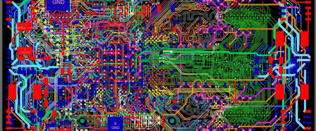
After the components are placed, the next step is routing. Routing involves connecting the components with traces that carry the electrical signals. It is important to minimize the length of the traces and reduce the risk of interference. It is also important to ensure that the traces are wide enough to carry the required current and that there is sufficient clearance between the traces to avoid short circuits. Careful attention should be paid to the placement of vias, which are used to connect traces on different layers of the board.
In summary, good PCB design requires careful consideration of the schematic design, component placement, and routing. By following these fundamental principles, you can create a reliable and effective circuit that meets the requirements of your project.
Signal Integrity

Grounding and Power Planes
Good grounding and power planes are essential for maintaining signal integrity in a PCB design. Grounding ensures that signals have a stable reference voltage, while power planes provide a low-impedance path for current flow. Here are some best practices for grounding and power planes:
- Connect all ground planes together to form a single, solid ground plane.
- Use multiple vias to connect ground planes on different layers.
- Keep the distance between the signal trace and the ground plane as small as possible.
- Use power planes instead of traces for high current connections.
- Place decoupling capacitors near the power pins of ICs to reduce noise.
Impedance Control
Impedance control is important for high-speed signals to prevent reflections and signal degradation. Here are some tips for impedance control:
- Use controlled impedance traces for high-speed signals.
- Keep the trace width and spacing consistent to maintain impedance.
- Use a ground plane under the signal trace to reduce crosstalk.
- Use a transmission line model to calculate the required trace width and spacing.
Signal Termination
Signal termination is necessary to prevent reflections and signal distortion. Here are some common types of signal termination:
- Series termination: A resistor is placed in series with the signal trace to match the characteristic impedance of the trace.
- Parallel termination: A resistor is placed in parallel with the signal trace to provide a low-impedance path for the signal.
- AC termination: A capacitor is placed in series with the signal trace to block DC signals and provide a high-impedance path for AC signals.
In conclusion, good signal integrity is critical for high-speed PCB designs. Proper grounding and power planes, impedance control, and signal termination are essential for maintaining signal quality and preventing noise and distortion.
Manufacturing Considerations
When designing a PCB, it is essential to consider the manufacturing process. A well-designed PCB can reduce manufacturing time, increase yield, and lower costs. Here are some important considerations to keep in mind during the manufacturing process:
Design for Assembly
Designing for assembly (DFA) is the process of optimizing a PCB’s design for ease of assembly. DFA can reduce assembly time and cost, improve product quality, and increase production yield. Some considerations for DFA include:
- Component placement: Grouping components by function and placing them in a logical order can reduce assembly time and minimize errors.
- Component spacing: Sufficient spacing between components can make assembly easier and reduce the risk of damage during the process.
- Orientation: Orienting components in a consistent direction can reduce assembly time and minimize errors.
- Soldering: Using surface-mount components and designing for automated pick-and-place machines can reduce assembly time and improve consistency.
Design for Testability
Designing for testability (DFT) is the process of optimizing a PCB’s design for ease of testing. DFT can reduce testing time and cost, improve product quality, and increase production yield. Some considerations for DFT include:
- Test points: Providing test points for critical signals can make testing easier and more accurate.
- JTAG: Using the Joint Test Action Group (JTAG) interface can simplify testing and reduce costs.
- Boundary scan: Using boundary scan can improve testing coverage and reduce test time.
- Built-in self-test (BIST): Incorporating BIST can reduce testing time and improve product quality.
Panelization
Panelization is the process of designing a PCB layout to fit within a larger panel. Panelization can improve manufacturing efficiency, reduce costs, and increase production yield. Some considerations for panelization include:
- Panel size: Choosing the right panel size can reduce material waste and increase production yield.
- Panel spacing: Sufficient spacing between PCBs can make assembly and testing easier and reduce the risk of damage during the process.
- Tooling holes: Including tooling holes in the panel can ensure accurate placement of the PCBs during assembly.
V-Score
V-scoring is the process of cutting a groove into the PCB to allow for easy separation after assembly. V-scoring can improve manufacturing efficiency, reduce costs, and increase production yield. Some considerations for V-scoring include:
- V-score depth: Choosing the right V-score depth can ensure easy separation without damaging the PCB.
- V-score spacing: Sufficient spacing between V-scores can reduce the risk of damage during the separation process.
- V-score alignment: Ensuring proper alignment of the V-score with the PCB layout can prevent damage to critical components.
By considering these manufacturing considerations during the design process, you can optimize your PCB design for ease of assembly, testing, and manufacturing, reducing costs, increasing yield, and improving product quality.
Design for Reliability
When designing a PCB, it is important to consider reliability. A reliable PCB design ensures that the circuit functions as intended, has a long lifespan, and is not prone to failure. Here are some factors to consider when designing for reliability:
Thermal Management
Thermal management is crucial for ensuring the longevity of a PCB. Components generate heat, and if the heat is not dissipated properly, it can cause damage to the components and the PCB itself. To ensure proper thermal management, consider the following:
- Use a ground plane to dissipate heat
- Place heat-generating components away from each other
- Use thermal vias to dissipate heat from the top layer to the bottom layer
- Use a heatsink for components that generate a lot of heat
EMI/EMC Considerations
Electromagnetic interference (EMI) and electromagnetic compatibility (EMC) can cause issues with the performance of a PCB. To minimize EMI/EMC issues, consider the following:
- Use a ground plane to reduce EMI
- Use shielded cables to reduce noise
- Place components that generate EMI away from sensitive components
- Use EMI/EMC filters to reduce noise
Component Selection and Placement
The selection and placement of components can have a significant impact on the reliability of a PCB. Consider the following:
- Use high-quality components from reputable manufacturers
- Avoid placing components too close together to prevent overheating
- Place components in a logical and organized manner to make troubleshooting easier
- Consider the accessibility of components for maintenance and repair
In conclusion, designing for reliability is essential for ensuring the longevity and proper functioning of a PCB. By considering thermal management, EMI/EMC considerations, and component selection and placement, you can create a reliable PCB that will perform as intended for years to come.
