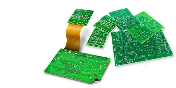
Different electronic devices in this digital world surround you. From your smart TV to your security camera, all devices have a PCB board at the heart of their design. All consumer electronics have PCB as the main component for functionality. PCB design evolved over the years, and their demand also grew.
The Printed Circuit Board (PCB) manufacturer has continued to grow to meet the pace of their demand, as every electronic device needs a printed circuit board. If you want to know about printed circuit boards, then you can find a lot of information by googling “printed circuit board.” But the flow of information regarding PCB design may need more clarification. Here we will provide a surface-level introduction to printed boards and PCB design.
Why Are Printed Circuit Boards Important?
Printed circuit boards are crucial for the functionality of modern electronic gadgets. Your electronic devices won’t be functional without printed circuit boards. PCBs are indispensable as they connect different components mounted on bare boards. They also make possible communication between them. Printed circuit boards protect these mounted components from damage and interference. So, when you use any electronic device, don’t forget to appreciate the device’s heart (printed circuit board). In simple words, printed circuit boards give life to electronic devices.
What Is Printed Circuit Board Design or PCB Design?
Printed circuit board designs are the basis of all electronic devices. Some PCB designs are simple, while some are more complex and harder to understand for a layman. At first sight, a printed circuit board design looks like a flat plate mounted with insulating materials that contain a pattern of conducting material and components.
CAD tools are quite popular in designing PCB layouts. These printed circuit board designs can be created manually and with automated software. Manual designs are created with the help of CAD tools drafting. Many sophisticated tools have automatic routers that help create the designs automatically.
PCB designers usually prefer the manual way of designing since they can implement their ideas and techniques in them. Still, many PCB designers use templates and integrate new circuits. Following PCB design basics and step-by-step guide will help you to design the best print circuit board.
Easy Steps for Printed Circuit Board Design
Why are PCB layout or design basics very important? Because when you are designing a product, PCB designs are equally important. If you are going to design PCB by yourself, the following steps will get involved from the initial drawings to the final design.
If you work with a competent electrical engineer and get involved, you finalize the best cost-effective printed circuit board PCB design. Otherwise, Multiple revisions can cost you both time and money. Let’s see what steps you should follow while designing PCB.
- You Must Know About Electrical Parameters and Symbols

The electrical parameters of the system play an important role during PCB design. So, you must be familiar with insulators, nets, Voltages, Capacitance limitations, Impedance, connectors, etc. you must have good know-how in designing tools and software for the board.
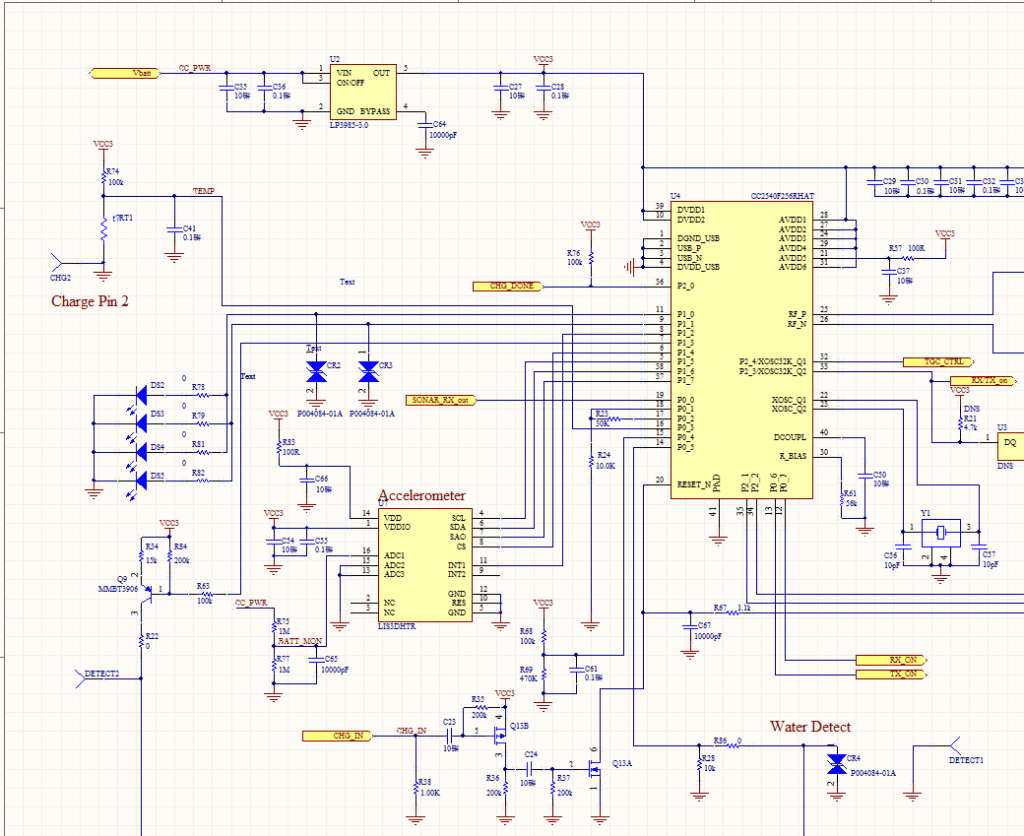
- Create The Schematic Diagram or Layout
Schematic capture is like blueprints for your new electronic device. The schematic layout is crucial whether you generate your PCB-designed form templates, use the Cad tool, or create your circuit board designed from scratch. First, your schematic layout helps you to know which components, such as capacitors, connectors, integrated circuits, etc., are going to be used in PCB design.
How are these components connected together on a PCB, and what is the relationship of these components with each other? You can roughly organize these parts to know the connectivity and later remove some parts to make the PCB design clear. Later you can add wires to connect the electric component, and the wire is known as nets.
- Verify That the Circuitry
When you organize all the components and nets on the schematic layout, the next important step is verifying the working for your Circuitry. Your circuit of PCB design should work in the desired way. For verification, you can use the circuit simulation tools. These tools allow PCB designers to test their circuits before building the actual hardware. In this way, they can know if there is any connection, if the net is not properly working or if something is faulty. Copper layers are in proper thickness.
Layout Components by using PCB design software. There are different designed software that is viable such as CAD tools, Autodesk EAGLE, Altium Designer, etc. The output of this design is usually in the form of a PCB schematic Gerber file. Gerber file encodes information, including copper tracking layers, drill drawings, component notation, and other parameters. Different software comes with different advanced features.
How to mount the components for their best performance and avoid areas of excessive heat and electrical noise are the things engineers gain with experience. Somehow modern tools can help you to avoid many pitfalls while designing printed circuit boards.
- Route The PCB Design
Different software has different features to connect the nets together. Some software has automated routing features that save a lot of time and energy. While routing, many things are kept into consideration, such as wire length that must be appropriate for proper conduct. Nets should not pass through the excessive noise area in this way, as they may degrade the performance of the PCB circuit board design.
It is crucial to make sure a clear PCB return. The Current Path must be clear and resistance-free to increase the efficiency of the board. If the surface has too many drill holes, cuts, or splits in them, then there is a chance of a lot of noise and reduced efficiency of PCB design. All the active electronic components on the board, such as ICs, conductors, and other components, need to be connected to power. The nets should be grounded.
- PCB Design Stack-Up
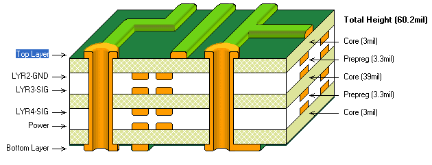
PCB design stack-up is crucial and requires a lot of attention. The copper layer and insulator’s specified arrangement make the PCB design stack up. Copper thickness also matters. It is necessary to pay attention to the PCB design stack-up before the final layout of the PCB board.
Multiple-layer PCB design increases the board’s ability to distribute energy. Multiple-layer PCB designs also reduce cross-interference and support high-speed signals. Good PCB stacking increases the efficiency of the product but also costs you less. A correct stack of PCB layers can improve the compatibility of the board with the final product. . The stack-up you choose certainly plays a vital role in the board’s performance in several ways. So always pay attention and do some work for the PCB design stack-up for better results. It is also crucial to pay attention to PCB design stack up due to impedance.
- Final Check for Rules
This is the last step to check whether your PCB circuit board design is according to the industry’s standard practices. Standards and acceptability criteria industry association. These standards and industry regulations tell you everything you need to know regarding PCB manufacturing. If you are not familiar with basic PCB design, solder paste, trace width, electronic circuits, etc., then find a professional PCB designer. They know industry practices and standards very well.
- Place Components and Drilling
It is time to build the board and send it for fabrication. Place all the components according to standard practices. Sometimes you have to make some changes in the PCB design board due to industry practices. Sometimes power and ground planes are problematic. Sometimes you can not place certain components with others due to resistance or noise, so you must make changes. The next step is drilling for the components and connectors; in the other step, route the traces. Usually, molten solder is used to create a permanent bond between different components.
- Labeling
It’s time to add labels and identifiers. You can add labels, and identifiers, to the component for convenience, as they show where specific components will go on the printed circuit board. These identifiers and designators for components are helpful during printed circuit board assembly. They also help if you need to debug or redesign your board for some reason.
- Generate Final Layouts
After routing to traces and labeling, it’s time to generate the final layouts. Once these files are generated, your PCB board design is ready for manufacturing and assembly. PCB assembly is another attention-seeking task.
By following the above steps, the process of creating a comprehensive PCB board design is as easy as counting to ten. Using a systematic approach such as this ensures that all aspects of your circuit board design are accounted for inherently during the process, with minimal need to retrace your steps.
- Use Up To Dated Printed Circuit Board Tools For The Best PCB Design.
The PCB design process is complex. The processes of PCB design and fabrication are tiring. It demands a lot of hard work and attention. It is crucial to work on Copper PCB design carefully to build a high-quality board; it is crucial to work on PCB design carefully. A precise PCB layout can bring the best PCB circuit board design for manufacturing.
So it is important to use the best PCB circuit board design tools for the best design. If you need a complex multiple-lay design, then select a tool carefully that must-have features and functionality. This must comprise dedicated features that help intricate route traces for high-speed circuits. These tools must have simulation features or tools to streamline all the processes and necessary testing. There are several advanced PCB board design tools already available in the market, and these tools can handle complex printed circuit board designs easily. So always choose the software or tools according to your PCB circuit board design and its layers.
Ideal Practice for PCB Circuit Board Design
The following are some ideal printed circuit board design practices.
- Choose A Skilled PCB Designer or Engineer.
Always choose a skilled PCB circuit board designer or engineer to get the best PCB circuit board design. It may cost you a bit high but never compromise quality over price.
PCB circuit board designer with extensive engineering experience knows all electrical parameters and is well-versed in industry practices. He knows the PCB design basics, the board outline, and all design rules. He knows how electronic components synchronize best. He is also capable of answering your queries and making a perfect design for you.
- Effective Communication
If you are availing the services of a PCB circuit board designer or engineer, then discuss everything openly with him. Tell him about your requirements for the PCB circuit board design and every other important detail regarding material, surface mount components, power, and ground planes. Effective communication with the PCB circuit board designer ensures you the best PCB circuit board design and reduces the chance of extensive revisions.
- There Is Always A Chance For Improvement.
Remember one thing: it is impossible to get a hundred percent accurate PCB circuit board design on the first attempt. There is always room for correction, change, or amendments. Effective communication ensures you get the best PCB circuit board design but don’t ignore the importance of necessary changes or revisions.
When you submit a design for fabrication and manufacturing, you must have all the necessary details like the right board size, the right component placement, power and ground planes, etc.
- Keep In Mind the Environment In Which The PCB Circuit Board Has to Function.
It is crucial to consider the environment in which the final design has to work while designing a PCB circuit board design. The weather circuit board is designed for extreme environments or non-extreme environments. If the PCB circuit board design is not compatible with the design, it will affect the efficiency of the circuit board. Dissipating heat is one of the biggest issues.
Types Of Printed Circuit Board Design Board
There are different types of circuit designs and PCB layouts. People use them according to product design.
- Single Layer PCB Design
These are simple PCB designs and PCB layouts that are easy to manufacture. They’re not complex integrated circuits and complex component placement. One side is covered with a copper layer, while the other side is the non-conductive substrate. Through-hole components are connected to the bare board.
- Double-Layer Printed Circuit Board PCB Designs.
A thin copper layer or copper foil is added on both sides in a double-sided PCB. Drill holes in the PCB allow electronic circuits and components to be connected. Double-sided PCB boards are mostly used in smartphones. In some complex devices, two circuit boards are also used.
- Multilayer Printed Circuit Board PCB Design.
The multilayer PCB design has three or more conductive layers. Two conductive copper layers are at the top and bottom, while another layer is sandwiched between non-conductive substrates. Multilayer PCB designs allow you to manufacture compact and smaller boards. The Multilayer PCB circuit manufacturing process is complex and requires high-density interconnect. The initial design has complex schematic symbols. Multilayer PCBs have complex electronic circuits. Net electrically connects the components.
- Rigid Printed Circuit Boards
The board’s base material is not common material, but it is a rigid substrate; these boards can be made in the single-layer design, double-layer design, and multilayer printed board circuit designs. High-density interconnects are mostly used in such types of boards.
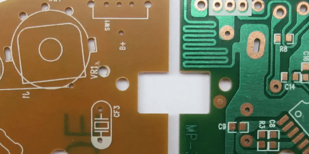
- Flexible Printed Circuit Boards
Flexible printed circuit boards are made up of many printed circuits and mounted components. Different components lead to electronic circuits. Flexible PCBs are greatly in demand due to their extensive use in laptops, LEDs, LCDs, etc. The top layer of this board is made of copper. The copper layer and components are arranged on a flexible substrate.
Disadvantages: A Poorly Designed Printed Circuit Board.
· A poorly designed PCB may require extensive revisions, which costs you both your time and energy. It is important to pass your PCB board design from the strict checklist to know the pitfalls of your designs.
· PCB circuit board designs aren’t inherently good or poorly designed. It’s a designer who made the worst PCB design. It’s the right use of a tool that creates an impact. If you know how to use these tools and software for the best-printed circuit board design, then they can be helpful in a multitude of ways. If not, you’ll only end up wasting your time and other resources.
· Inspecting the board’s layout to eliminate as many issues as possible that could arise during the assembly process. DFM is there to ensure the result is a functioning PCB. A poorly designed printed circuit board can affect the electrical performance of the signal transmission, and your product may not work efficiently.
· It would not result in the required efficiency or productivity. It also affects the long-term reliability and durability of the finished product.
Common Myths About Printed Circuit Board Design
Time has changed, and technology has brought a revolution in every field. Printed circuit board designs are easy to make and more practical nowadays. Many old techniques and tips are obsolete nowadays. Following are some myths regarding printed circuit boards that you must bust while designing your printed circuit board.
- Be Creative and Start from Scratch.
Don’t start from scratch while designing printed circuit boards. It’s high time to work smartly in every field then why not in printed circuit board designs? Whenever you start printing circuit boards, then there is no need to start from scratch. Many of the components you need to make the circuit boards already exist and are used in other devices.
So, why waste a lot of time and energy doing something that is already done? Go through the archive of printed circuit board designs. You can find the designs you need, and with little changes, you can use them in your current PCB project. You just have to make a few circuits or changes. Now your job is simpler and faster.
- Don’t Use Ninety Degree Angles.
Avoiding ninety-degree angles in printed circuit board design was the golden rule. It is used as a tip in printed circuit board design class. Many old-school engineers and designers give you this pro tip, and to some extent, it has logic. Many outdated printed circuit board design tools were unable to handle ninety-degree angles well.
Acid can collect in those ninety-degree corners. These ninety-degree angles cause etching problems in practical work. That’s why forty-five-degree angles have been the preference. Modern engineers use alkaline etching nowadays, eliminating acid traps. Recent top-notch tools and software work well with ninety-degree angles. It is necessary to keep updated your printed circuit board designing tools.
- Ban on Via in Pad.
Another golden piece of advice you may hear while designing a PCB circuit board is to avoid via in-pad. According to old school Printed circuit board designers, it was a sin. Soldering a pad into place, a via hole in your printed circuit board design can cause several issues, such as copper traces and hard integration of circuits and component placements.
So many old PCB manufacturers don’t accept the PCB design via in-pad. Nowadays, in modern PCB design, making via in-pad increases the efficiency of circuit board design. It can help with dissipating heat and ground plane problems. So, if you get into the mindset of just not using via in-pad, you may land in too many problems. Now modern PCB design tools allow you to have a via in pad. It is necessary to keep yourself updated with the latest printed circuit board design tools and modern techniques. If you are not familiar with new software or tools, then you must learn them to make the best PCB design.
Wrapping Up the Things
In Today’s fast electronic world, PCBs are essential to all devices. That’s why it is necessary to pay careful attention to PCB designs and industry practices. With growing demand and innovative products, printed board designs are getting the status of art. The global growth of the PCBs market is driven by the increased use of multiple layers and metal core boards. The board size and design complexity keep increasing with more innovative devices. If you are not skilled enough to design a PCB, then take services from a professional engineer.
