Defects or manufacturing-induced errors are prone to crop up at different times during the production process of different products. When it comes to electronic device production, it happens when the soldering process wasn’t completed in the due way.
Solder ball and bridging defects tend to come up in this case and the way you handle it has an impact on the PCB’s performance. This is why we dedicate this article to explaining the concepts of ball soldering and bridging, as well as proffering solutions on how to avoid these issues.
Solder Ball and Solder Bridging: Two Different Concepts
It is pertinent to clarify that solder ball is different from solder bridging so you don’t confuse them to be the same.
However, they are some of the common defects you can spot on your PCB.
What is Solder Ball?
Also called ball soldering or solder balling, it is a PCB defect or design error that leads to the formation of small balls of solder on the PCB’s surface during the soldering process.
It is possible for the solder balls to be attached to a pad or component on the PCB. It is also possible to have it on a standalone – not attached to anything, but still sitting there on the circuit board’s surface.
What Causes Solder Ball?
It is easy to identify a solder ball due to the small shape it takes, which often turns into a ball-like shape. But, what really causes ball soldering on a PCB?
Here are a few pointers:
Solder Paste Smear
The solder ball is formed from a solder. Therefore, if you mistakenly smeared the solder paste, especially when working on the stencil’s bottom side during the printing process; the likelihood of balling is high.
Flux Activation Failure
The failure of the flux to activate during the preheat period can lead to ball soldering. It is important to mention that the activation failure can be caused by any of the following:
- The preheat temperature is not high enough.
- If heat is not applied at all during the initial stages of soldering.
Excessive Solder Paste
The presence of excessive or more-than-required solder paste that is being expelled around the SMD pad leads to ball soldering. The concept is called paste expulsion.
When this happens, it is because of any of the following factors:
- High pressure during placement
- Misregistration also causes paste expulsion near the Surface Mount Device (SMD) pads.
Printing Misalignment
A misalignment or mispositioning of where the solder paste is to be printed could be the issue. In this case, printing the solder paste (for instance), on the solder mask instead of the SMD pad could lead to solder balling.
Excess Moisture
An excessive presence of moisture could lead to what is called moisture contamination. Commonly tenable during the reflow process when the initial preheat temperature is low; it often leads to solder paste migration.
Other possible causes of solder balling are:
- Excessive placement pressure potentially leads to squeezing the solder paste out of the pads.
- It is possible to have solder balling after selective soldering, whereby insufficient cleaning and wiping post-reflow process is tenable.
Possible Corrective Measures for Solder Balling

Seeing that ball soldering on a PCB is usually one of the reflow soldering defects, we can move to resolve the issues in the following ways:
Preheat the PCB
It is important to put the circuit board to a preheat whereby it will get “familiarized” with the oven’s temperature.
In addition to enabling an even melting of the solder paste, the preheating stage also reduces the chances of negative changes when the main heating phase commences.
Check the Circuit Board’s Thickness
The thickness of the PCB should be checked, as that allows for the increased quality of the circuit board.
For emphasis, the thickness of the board’s hole plating copper should be above 25µm. Sticking to this standard helps reduce the risks of moisture getting trapped inside the PCB.
Follow the Design Rules
Designing both the pad sizes and spaces is important, as it helps you stick to the information in the datasheet.
Stencils Must be Cleaned
One reason why ball soldering happens on a PCB is because of the residue trapped inside the circuit board’s pads and surfaces.
Therefore, you must endeavor to either flux off the excessive solder paste left on the stencil or clean/wipe off the same, properly.
Get Rid of Moisture in the PCB
Moisture of any form shouldn’t be trapped inside the circuit board. Getting rid of the same is a priority, as leaving moisture behind tends to aggravate the risk of ball soldering.
Here are some tips on how to get rid of excessive moisture inside a PCB:
- Be sure to dry-off dampness on the boards before working on them. You can use anti-static cloths for this purpose.
- You can also make a manual evaporation by storing the PCBs in a dry environment.
- If you notice moisture or dampness inside the PCB and it is something you cannot manually handle, consider preheating the board. You can bake it up to 120˚C to help remove the trapped moisture.
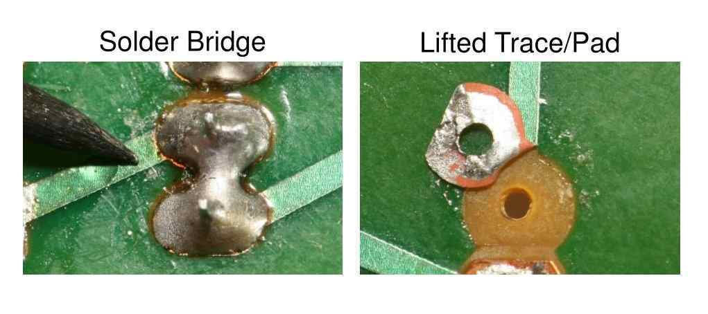
What is Solder Bridging and How Does It Affect PCB’s Performance?
On the other hand, solder bridging is different from the solder balling because it has to do with the creation of electrical shorts that lead to malfunctioning of the circuit, electric-wise.
Also called electrical bridging, solder bridging happens when an unintended connection of solder forms between two traces, pins or pads. This formation leads to the formation of a conductive path that culminates in short-circuiting.
Potential Causes of Solder Bridging in a PCB
Several factors can cause a solder to bridge in a Printed Circuit Board (PCB). However, the basic point to have in mind is that the bridging happens because of the smaller footprints of modern electronic devices, which leads to limited spaces. Thus, there is a likelihood of using a solder paste across two conductors that ought not to be connected, electrically.
With that being said, here are some possible causes of electrical bridging in a circuit board:
- Component misalignment, especially when these parts are being placed on the PCB.
- Solder bridging happens when there is no solder resist/mask between the adjacent pads.
- A PCB begins to have electrical bridging when there are residues stuck on either the PCB pads or surfaces – or even the both.
- Excessive solder paste application to the pads can be a cause.
Solutions for Solder Bridging Defects on a PCB
You can resolve the solder paste printing defects by using a solder mask or solder resist to prevent solder from getting to the places it is not required on the PCB. Another way to resolve the solder paste-induced defects is by applying an appropriate solder paste metal to flux weight ratio.
The following are additional ways to resolve solder bridging issues on a PCB:
- The appropriate pad-to-pad spacing should be maintained. The same spacing should be maintained when applying solder mask between these pads.
- The stencil should be cleaned to prevent the presence of residues.
- Old and new flux should not be mixed and used together.
- The zero-print gap between the stencil and the circuit board should be zero.
Conclusion
Printed Circuit Boards (PCBs) are prone to several issues, errors and manufacturing defects. Aside from solder balling and electrical bridging, other common errors are: dewetting solder, tombstoning, insufficient fills and solder beading.
In light of these errors, you can avoid some of the common solder wetting issues and other design challenges if you had your PCB designed at a reliable manufacturing company. Contact us today with your PCB specifications and let us do the best we can to prevent your circuits from balling or bridging due to excessive solder paste usage or mismanagement.
