Applying a solder resist to the Printed Circuit Board (PCB) can make a lot of impact to how the circuit board’s protection is guaranteed. For some consumers, it is a lot of deal for the circuit board and the associated components to be maximally protected.
In this article, we give you a detailed insight into what the PCB solder resist is all about, as well as some of the important points to the functionality.
What is PCB Solder Resist?
First, let us break down the two terms – solder and resist. The former has to do with a material called solder and the other is the action of that material, which is resistance.
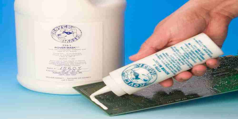
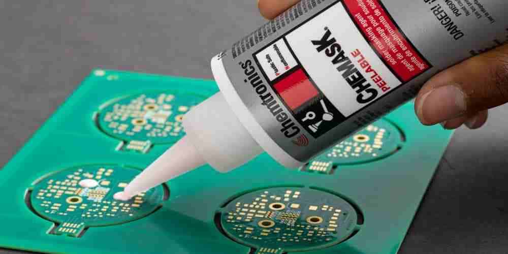
Simply put, a solder resist is an insulating ink used to cover the surface of Printed Circuit Boards (PCBs). The reasons why this is important will be discussed later in this post.
Composition of the Solder Resist
You will realize that most PCBs with solder resist have it as a green colour. While this is the standard or what has become prevalent; it is also possible to have it in other colours.
The following are some of the options for the solder resist, in terms of the colour or outlook:
- Pink solder resist
- Blue solder resist and;
- Red solder resist
These colours refer to the type of ink used for the covering. Also, the performance of the ink might not be different, even if they are presented in other colours, other than green.
Functions of Solder Resist on a PCB
The following are some of the major roles or functions of the solder resist when it is applied to the circuit board’s surface:
1. Overall Protection
Besides covering the PCB’s surface, the solder resist also protects the circuit pattern. It is important to mention here that the protection is often restricted to the important (conductive) areas of the PCB. For this to work, the ink is used to cover and isolate these conductive areas as a way of preventing them from exposure to the non-conductive areas.
2. Solder Adhering Protection
Due to the fact that solder can adhere or shift to some of the unnecessary areas in the PCB, applying solder resist could go a long way to prevent that.
Solder resist’s function in this regard is to prevent the solder from adhering or derailing to the unnecessary areas other than the locations of the electrical contacts on the PCB.
In light of this function, it is impossible for the solder to trigger issues like short-circuiting, especially when multiple components are soldered or attached to the PCB’s surface.
3. Circuit Pattern Insulation
The pattern of the Printed Wiring Board (PWB) is maximally protected with the aid of solder resist. This is an important innovation, owing to the fact that modern electronic devices use a smaller footprint/real estate.
By insulating the circuit pattern, the solder resist helps the PCB to stick to the method of miniaturization, which promotes thinner footprints.
4. Contaminants’ Protection
Protecting both the surface and pattern of PCBs also goes a long way to prevent contaminants, such as moisture, heat and dust from penetrating into the board’s circuitry.
5. Coating Performance
The coating or application of the solder resist ink on the PCB’s surface helps in the protection of the circuit pattern in two different ways.
For the first benefit, it helps to protect the coated circuit pattern from the dangers of breaking and short-circuiting. It also provides sufficient insulation for the PCB’s pattern.
The second benefit is that the non-coated areas are not left out. To this end, the solder resist helps to provide the necessary contacts that allow for the electrical connections to be made for component mounting.
6. Improved Reliability
In addition to acting as a protective layer for the PCB, the solder resist ink also helps to improve the board’s reliability. This is tenable due to the protection of the board and its pattern from the contaminants and harmful agents that could have negatively impacted the performance.
Choosing the Best Solder Resist Material

A variety of options are open to you when choosing a solder resist for your PCB. An understanding of how each of these works and when best to apply them is a plus.
Here are some of the common types of solder resist you can choose:
1. Liquid Ink Photoimageable Solder Resist
This is also called the Liquid Photoimageable Solder Mask (LPSM). It is a type of solder resist made of an ink formulation.
The following points define how the LPSM or LPI solder resist works:
Application Process
There are three (3) different ways you can maximize the use of LPI process for solder resist application. The first method is by silkscreening it. In addition to being one of the most affordable processes, it also requires the mixture of the liquid components before application, as doing this increases the shelf life.
The second process is by spraying the solder resist ink over the circuit board’s surface. Just as this method is affordable, it also demands an exposure to the pattern before the development.
The third application process for the LPI solder resist method is by using the lithography process. This is an advanced method and it comes with the perks of helping in the definition or specification of the solder mask openings for the mounting holes, pads and vias.
UV Exposure
The LPSM or LPI solder mask application method is sensitive to the Ultraviolet (UV) light. To this end, careful measures must be taken when making the exposure.
Here are some of the best practices for exposing the board to UV light:
- The solder resist or solder mask can be aligned over the dried circuit board and exposed to UV light. This should come after the circuit board has been dried in an oven.
- The unexposed areas of the circuit board have to be washed off with a solvent or dedicated solution. This helps the unrequired areas to be taken off, thus, leaving behind the hardened layer of solder resist.
- Developers, which are high-pressure water sprays, can be used to remove the solder resist.
- To finalize the process, organic coating and thermal curing should be used to “finish” the circuit board.
2. Liquid Epoxy Solder Resist
Also called the epoxy liquid solder resist/mask, they are the solder resist type that requires the use of silkscreen processes to make an imprint of epoxy over the circuit board.
The following details underscore the silkscreen printing process for epoxy liquid solder masks:
- A woven mesh is used to support either the ink-blocking patterns or ink-blocking stencils.
- The woven mesh is also used to create open areas in the PCB’s surface. these areas pave the way for ink to be spread or transferred to the relevant places on the surface.
- Thermal curing is often used as the finishing process for liquid epoxy solder masks.
For the best results when working with the solder resist inks on epoxy liquid solder masks, the following measures must be observed:
- Epoxy liquid should be used for the process. It is a thermosetting polymer, which hardens when the PCB is subjected to thermal curing.
- To derive the best colour, the solder mask dye should be mixed into the liquid epoxy.
3. Dry Film Solder Resist
This is also called the Dry Film Solder Mask (DFSM). It refers to the use of dry film for the process.
Here are some of the things you need to know about the dry film solder resist process:
Vacuum Lamination Process
Dry solder resist film supports the use of a vacuum lamination process. The process supports the application of the dry film in the form of sheets of solder mask film.
The benefits of choosing the vacuum lamination process over liquid application include:
- It helps to remove bubbles from the dry film.
- The lamination process is effective towards the enforcement of the unexposed solder resist film’s resistance to adhere to the circuit board.
The completion of the vacuum lamination process leads to the exposure and development of the circuit board.
Soldering and Layering
The completion of the exposure and development process leads to the soldering and layering process. At this stage, openings will be made in the PCB’s pattern. These openings are the pathway for the components or parts to be soldered to the copper pads.
An electrochemical process is used for the layering. To work effectively, copper will be layered both inside the holes on the board and on the trace areas.
The copper circuits’ protection is enhanced by the application of tin.
The Curing Process
Before the curing begins, the dry film is removed and etched marks on the copper are exposed. Thermal curing is often used to finalize the process.
4. Top-and-Bottom-Side Solder Resist
This refers to the type of solder resist used for identifying or recognizing the openings in the green solder resist layer.
Here are some important points to note about this method:
- The solder resist material can either be placed on the top or bottom of the PCB.
- Either the film or epoxy methods can be used to make a pre-addition of the green solder resist layer.
- The openings registered with or created with the masks are used to solder the component pins.
Conclusion: Is Solder Resist Different from Solder Mask?
No, they are one and the same. Solder resist is known by other names, such as solder mask. The role of the solder resist includes protecting the copper traces and the interfaces between them on the PCB’s surface, as well as acting as a primary protection against corrosion, and oxidation.
Hillman Curtis is a leading manufacturer of circuit boards with solder resist capabilities. We optimize the solder masks, as per the applications you want to use the PCBs for.
