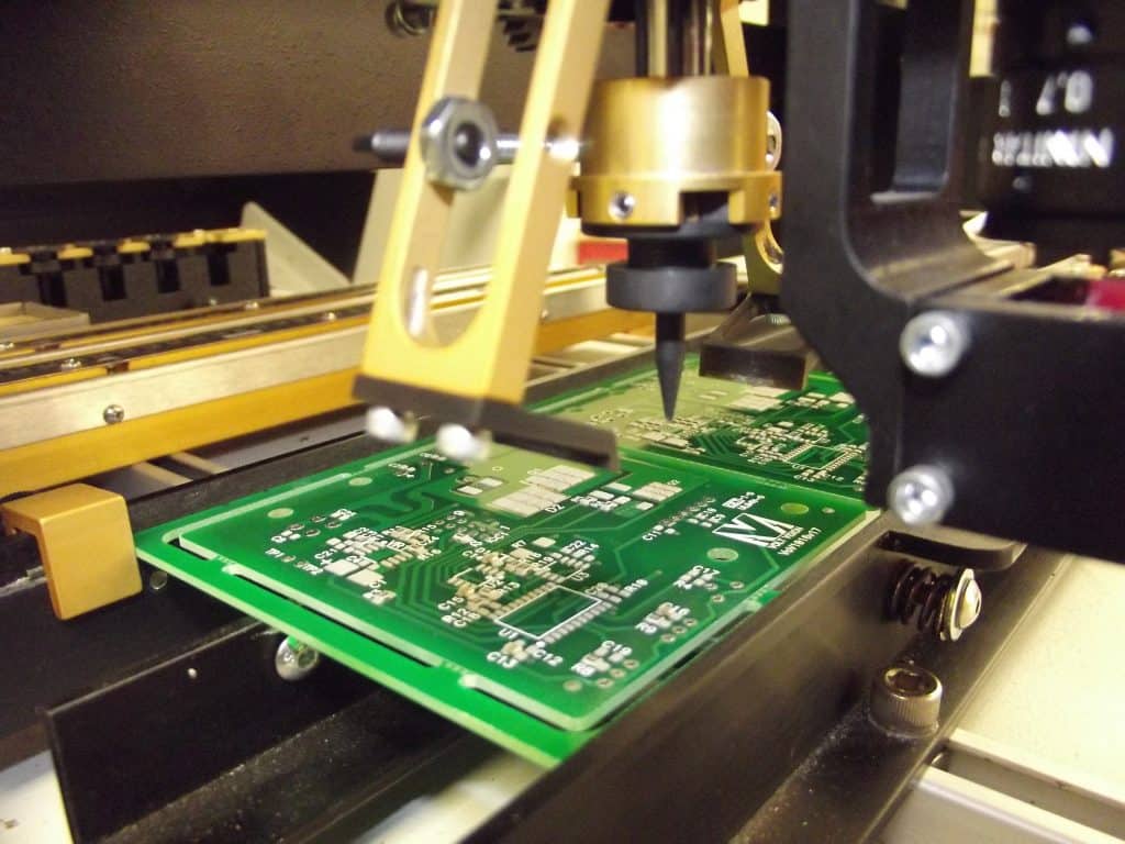
KiCad is a popular open-source software suite for electronic design automation (EDA). It includes a schematic editor, a PCB layout editor, and a 3D viewer for PCB design. KiCad is available for Windows, Linux, and macOS, and it is used by hobbyists, students, and professionals alike.
The KiCad layout editor is a powerful tool for designing printed circuit boards (PCBs). It allows users to create a layout for their circuit, place components, and route connections between them. The software also includes tools for checking the design for errors, generating manufacturing files, and exporting 3D models of the PCB. With KiCad, users can create professional-quality PCBs without the need for expensive proprietary software.

Overview
What is KiCad Layout Editor?
KiCad Layout Editor is a free, open-source software tool used for designing printed circuit boards (PCBs). It is a part of the KiCad suite, which also includes schematic capture and Gerber file generation tools. KiCad Layout Editor is available for Windows, Linux, and macOS.
The software provides a user-friendly interface for designing PCBs. It includes a variety of features, such as a 3D viewer, design rule checking, and automatic routing. KiCad Layout Editor uses a powerful engine that can handle complex designs with ease.
Features
KiCad Layout Editor offers a range of features that make it a popular choice for designing PCBs. Some of the key features include:
-
Multi-sheet schematic support: KiCad Layout Editor allows users to design complex circuits by creating multiple sheets of schematics.
-
Design rule checking: The software includes a design rule checker that ensures that the PCB design meets the required specifications.
-
Automatic routing: KiCad Layout Editor can automatically route traces on the PCB, saving time and effort.
-
3D viewer: The software includes a 3D viewer that allows users to visualize their PCB designs in three dimensions.
-
Footprint editor: KiCad Layout Editor includes a footprint editor that allows users to create custom footprints for their components.
Overall, KiCad Layout Editor is a powerful and versatile tool for designing PCBs. Its user-friendly interface and range of features make it a popular choice for both hobbyists and professionals.
Getting Started

Downloading and Installing KiCad Layout Editor
To get started with KiCad Layout Editor, you’ll first need to download and install it on your computer. The software is available for free on the KiCad website and is compatible with Windows, Mac, and Linux operating systems.
Once you’ve downloaded the software, simply follow the installation prompts to complete the installation process. Note that the installation process may vary slightly depending on your operating system.
Creating a New Project
To create a new project in KiCad Layout Editor, open the software and select “File” from the top menu bar. Then, select “New Project” from the drop-down menu. From there, you’ll be prompted to name your project and select a location on your computer to save it.
Once you’ve created your project, you’ll need to add schematic files to it. To do this, select “File” from the top menu bar again and select “Add Files” from the drop-down menu. From there, you can select the schematic files you want to add to your project.
Navigating the User Interface
The KiCad Layout Editor user interface can be a bit overwhelming at first, but it’s actually quite intuitive once you get the hang of it. The main window is divided into several different sections, including the schematic editor, the layout editor, and the library editor.
To switch between these different sections, simply click on the corresponding tab at the top of the window. You can also use the toolbar at the top of the window to access various tools and functions, such as adding components to your schematic or adjusting the layout of your PCB.
Overall, KiCad Layout Editor is a powerful and versatile tool for creating electronic schematics and PCB layouts. With a bit of practice, you’ll be able to create professional-quality designs in no time.
Designing a PCB Layout
Creating Schematics
Before designing a PCB layout, it is important to create a schematic. The schematic is a visual representation of the circuit you want to build. KiCad provides a schematic editor for this purpose. You can add components, connect them with wires, and label them as necessary. The schematic editor also has built-in tools for checking the electrical connectivity of your circuit.
Placing Components
Once you have created the schematic, you can move on to placing components on the PCB layout. KiCad provides a footprints library with a wide range of components that you can use. You can also create your own custom footprints if necessary. It is important to place components in a logical and organized way to ensure that the final product is easy to manufacture and repair.
Routing Traces
Routing traces is the process of connecting the components on the PCB with copper traces. KiCad provides tools for routing traces manually or automatically. It is important to ensure that the traces are of the correct width and spacing to avoid signal interference. You can also add vias to connect traces on different layers of the PCB.
Adding Text and Graphics
Adding text and graphics to the PCB layout can help to make it easier to understand and manufacture. KiCad provides tools for adding text labels, logos, and other graphics to the PCB. It is important to ensure that the text and graphics are clear and easy to read.
In conclusion, designing a PCB layout using KiCad is a straightforward process. By following the steps outlined above, you can create a professional-looking PCB layout that is easy to manufacture and repair.
Design Rule Checking
Setting Up Design Rules
Before running a Design Rule Check (DRC), it is important to set up the appropriate design rules. This can be done in the “Design Rules” dialog box, which can be accessed by clicking on “Design Rules” in the top toolbar.
In the dialog box, you can set up rules for various aspects of your design, such as minimum trace width, clearance between traces, and minimum drill size. You can also set up specific rules for different layers of your design.
It is important to carefully consider the design rules you set up, as they will affect the manufacturability and reliability of your board. Consult the manufacturer’s specifications and guidelines to ensure your design rules are appropriate.
Running Design Rule Checks
Once your design rules are set up, you can run a Design Rule Check (DRC) to ensure your design meets those rules. To run a DRC, click on “Tools” in the top toolbar, then select “DRC” from the dropdown menu.
The DRC will check your design against the rules you have set up and highlight any violations. You can review the violations in the “Messages” panel, which can be accessed by clicking on “Messages” in the bottom toolbar.
It is important to carefully review and address any violations before sending your design for manufacturing. Ignoring violations can result in manufacturing errors, poor performance, and even damage to the board.
In conclusion, setting up and running a Design Rule Check is an essential step in the PCB design process. By carefully considering and implementing appropriate design rules, and thoroughly reviewing any violations, you can ensure a high-quality, reliable board.
Exporting and Manufacturing
Generating Gerber Files
To export your KiCad design for manufacturing, you need to generate Gerber files. Gerber files are the industry-standard file format used by PCB manufacturers. The Gerber files define the copper layers, solder mask, silkscreen, and other details of your design.
To generate Gerber files in KiCad, go to File > Plot. In the Plot window, select the layers you want to include in your Gerber files. You should include all copper layers, solder mask, and silkscreen layers. You can also include drill files and board outline files if necessary.
Once you have selected the layers, click on the Plot button. KiCad will generate the Gerber files in the folder you specified. Make sure to review the Gerber files carefully before sending them to the manufacturer to ensure that they match your design.
Sending Files to a Manufacturer
After generating the Gerber files, you need to send them to a manufacturer for PCB fabrication. Most manufacturers have an online order form where you can upload your Gerber files and specify the board details, such as board thickness, copper weight, and solder mask color.
Before sending your files to the manufacturer, make sure to review their design rules and requirements. The manufacturer may have specific requirements for the Gerber files, such as the number of layers, drill sizes, or board dimensions. You should also check the manufacturer’s turnaround time and pricing to ensure that they can meet your requirements.
In addition to the Gerber files, you may need to send other files to the manufacturer, such as a bill of materials (BOM) and a pick and place (PnP) file. The BOM lists all the components used in your design, while the PnP file specifies the location and orientation of each component on the board.
Once you have uploaded your files and specified the board details, you can submit your order to the manufacturer. The manufacturer will review your files and contact you if there are any issues or questions. After the manufacturer has fabricated your PCB, they will ship it to you, and you can begin assembling your project.
Remember to double-check all your files and specifications before submitting your order to the manufacturer. Any errors or mistakes can delay the fabrication process and result in additional costs.
