Printed Circuit Boards (PCBs) are crucial components in the design of electronic circuits. They provide a platform for the components to be mounted on and connected together to form a functional circuit. In the design of DC to AC inverters, PCB layout plays a critical role in the performance and reliability of the circuit.
The PCB layout for a DC to AC inverter involves the placement and routing of the components on the board. The layout must be carefully designed to ensure that the circuit operates efficiently and reliably. The placement of components must be optimized to minimize noise and interference and ensure proper heat dissipation. The routing of the traces must be carefully planned to minimize signal distortion and ensure proper grounding.
Basics of PCB Layout
When designing a PCB for an inverter DC to AC, it is important to consider the layout to ensure proper functionality and performance. The layout should be optimized to minimize noise, reduce the risk of errors, and allow for efficient assembly. The two key aspects of PCB layout are component placement and routing.
Component Placement
Component placement is critical to the overall performance of the inverter. It involves determining the optimal location for each component to ensure that it is properly connected to other components and that the signal paths are as short as possible.
To achieve optimal placement, it is important to consider the following factors:
- The size and shape of the components
- The location of the power supply and ground
- The orientation of the components
- The thermal considerations
A well-placed component can reduce the noise and improve the signal integrity of the inverter.
Routing
Routing refers to the process of connecting the components together to form a functional circuit. It involves laying out the traces, vias, and pads to ensure that the signal paths are short, direct, and efficient.
To achieve optimal routing, it is important to consider the following factors:
- The location of the components
- The number of layers in the PCB
- The size and shape of the traces
- The spacing between the traces
- The thermal considerations
A well-routed PCB can reduce the noise and improve the signal integrity of the inverter.
In conclusion, the basics of PCB layout for an inverter DC to AC involve careful consideration of component placement and routing to ensure proper functionality and performance. By optimizing the layout, it is possible to reduce noise, minimize errors, and improve the overall quality of the inverter.
Considerations for Inverter Circuit

DC Input Circuit
When designing an inverter circuit, the DC input circuit is an important consideration. The input voltage, current, and waveform must be carefully selected to ensure that the circuit operates efficiently and safely.
One important consideration is the voltage level of the DC input. The inverter circuit must be designed to handle the voltage level of the DC input, which may range from a few volts to several hundred volts. This will depend on the specific application and the power requirements of the inverter.
Another consideration is the current rating of the DC input circuit. The circuit must be designed to handle the maximum current that will be drawn by the inverter. This will depend on the power rating of the inverter and the load that it will be driving.
Finally, the waveform of the DC input must be considered. The inverter circuit must be designed to handle the specific waveform of the DC input, which may be a pure DC waveform or a pulsating DC waveform.
AC Output Circuit
The AC output circuit is another important consideration when designing an inverter circuit. The output voltage, current, and waveform must be carefully selected to ensure that the circuit operates efficiently and safely.
One important consideration is the voltage level of the AC output. The inverter circuit must be designed to produce the correct output voltage level for the specific application and load that it will be driving.
Another consideration is the current rating of the AC output circuit. The circuit must be designed to handle the maximum current that will be drawn by the load.
Finally, the waveform of the AC output must be considered. The inverter circuit must be designed to produce the specific waveform required by the load, which may be a pure sine wave, a modified sine wave, or a square wave.
In summary, when designing an inverter circuit, careful consideration must be given to the DC input circuit and the AC output circuit. These circuits must be designed to handle the specific voltage, current, and waveform requirements of the application and load.
Designing the Inverter Circuit
Schematic Design
The first step in designing an inverter circuit is to create a schematic diagram. This diagram will show the overall circuit layout and the connections between the various components. The main components of the inverter circuit are the DC power source, the oscillator, the driver circuit, and the power transistors.
The DC power source provides the power for the inverter circuit. The oscillator generates a square wave signal that will be used to drive the power transistors. The driver circuit amplifies the signal from the oscillator and provides the necessary current to drive the power transistors. The power transistors switch the DC power source on and off to create an AC output.
When designing the schematic diagram, it is important to choose components that are suitable for the intended application. The selected components should be able to handle the required power levels and have the necessary voltage and current ratings.
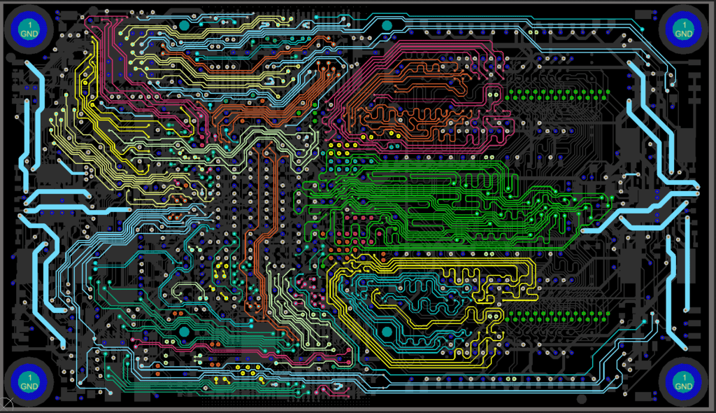
PCB Layout Design
Once the schematic diagram has been created, the next step is to design the PCB layout. This involves determining the physical placement of the components on the PCB and designing the traces that will connect the components.
When designing the PCB layout, it is important to keep in mind the electrical characteristics of the circuit. The placement of components and the routing of traces can have a significant impact on the performance of the circuit. It is important to minimize the length of the traces and to avoid crossing traces to reduce the risk of interference.
The PCB layout should also take into account the physical constraints of the application. The size and shape of the PCB should be designed to fit within the available space and to accommodate any mounting requirements.
In summary, designing an inverter circuit involves creating a schematic diagram and designing the PCB layout. The schematic diagram shows the overall circuit layout and the connections between the components. The PCB layout determines the physical placement of the components and the routing of the traces. Careful consideration of the electrical and physical characteristics of the circuit is necessary to ensure optimal performance.
Testing and Troubleshooting
Testing the Inverter Circuit
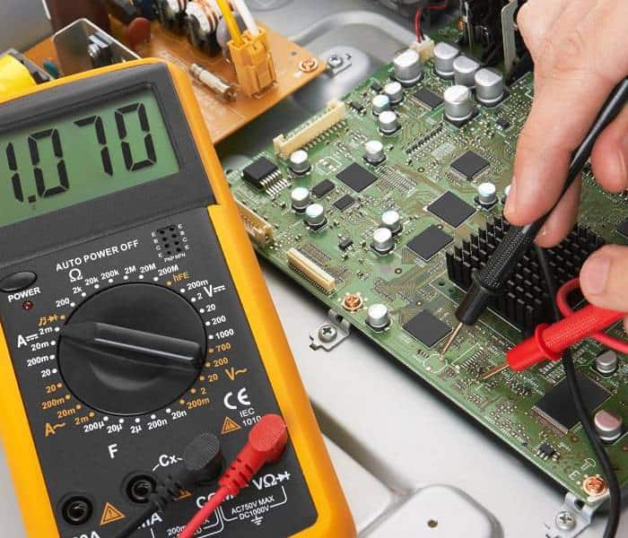
To test the inverter circuit, you can use a multimeter to measure the output voltage of the inverter. Connect the positive probe of the multimeter to the output terminal of the inverter and the negative probe to the ground terminal. Turn on the inverter and measure the output voltage.
If the output voltage is not within the expected range, check the input voltage to the inverter. Make sure it is within the specified range. Also, check the connections between the inverter and the battery. Loose or corroded connections can cause voltage drops and affect the performance of the inverter.
Troubleshooting Common Issues
If the inverter does not turn on, check the battery voltage and make sure it is above the minimum required voltage. Also, check the fuse and replace it if necessary.
If the inverter turns on but does not produce any output, check the input voltage and make sure it is within the specified range. Also, check the connections between the inverter and the battery.
If the inverter produces output but the voltage is too low or too high, check the input voltage and make sure it is within the specified range. Also, check the load connected to the inverter and make sure it is within the rated capacity of the inverter.
In case of any other issues, refer to the manufacturer’s manual for troubleshooting tips and contact their support team if necessary.
