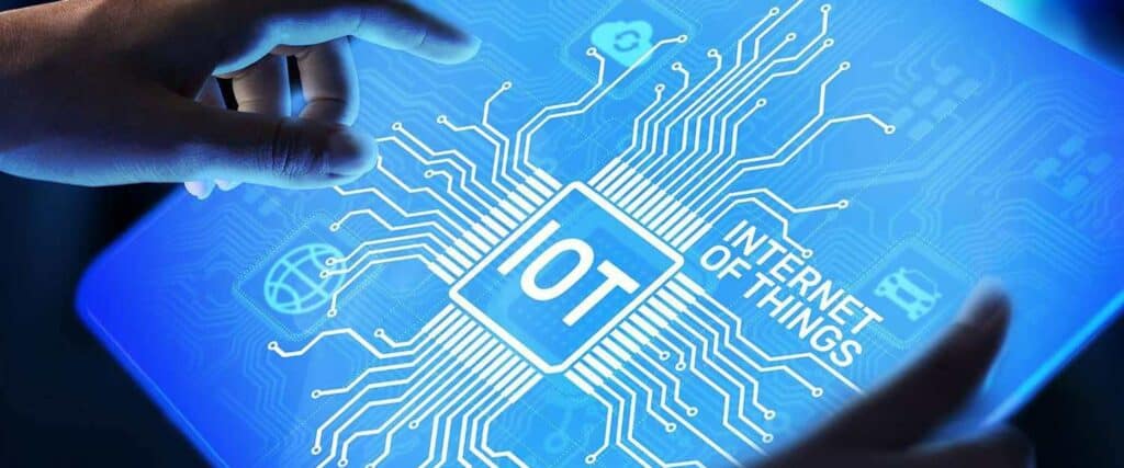
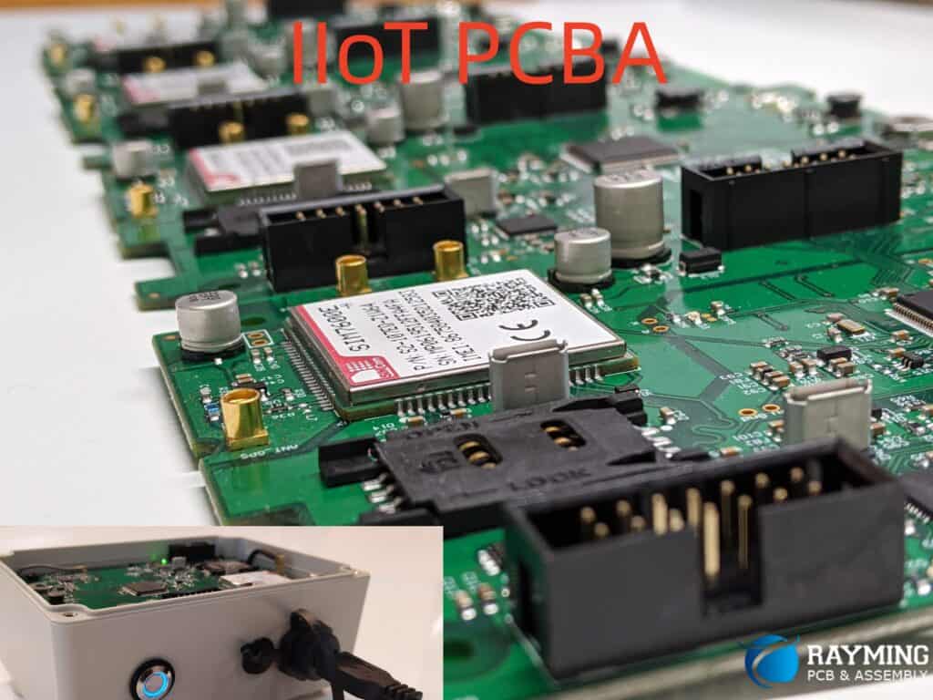
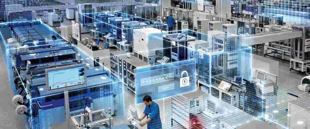
Printed circuit boards (PCBs) are an essential component of IoT devices. They are the backbone of the electronic circuits that power IoT devices, connecting various electronic components and enabling them to communicate with each other. PCBs are used in a wide range of IoT applications, including smart homes, wearables, industrial automation, and smart cities.
Manufacturing PCBs for IoT devices requires specialized knowledge and expertise. The process involves designing the circuit board layout, selecting the appropriate components, and assembling the board using advanced manufacturing techniques. The manufacturing process must be precise and consistent to ensure that the PCBs meet the required specifications and are reliable and durable. In addition, PCBs for IoT devices must be designed to meet the unique requirements of each application, such as low power consumption, high data transfer rates, and resistance to harsh environmental conditions.
Overall, the manufacturing of PCBs is a critical aspect of the IoT industry, enabling the development of innovative and reliable devices that are transforming the way we live and work. As the demand for IoT devices continues to grow, the manufacturing of PCBs will play an increasingly important role in the development of new and exciting applications.
Benefits of Manufacturing Printed Circuit Boards in IoT
Manufacturing Printed Circuit Boards (PCBs) in IoT has several benefits. Here are some of them:
-
Cost-effective: IoT devices require PCBs with specific designs and functionalities. Manufacturing PCBs in IoT can reduce costs by eliminating the need for manual labor and minimizing material wastage. With the help of IoT, PCBs can be produced in large quantities at a lower cost.
-
Improved Quality Control: IoT-enabled PCB production allows for real-time monitoring of the manufacturing process. This ensures that the PCBs are manufactured to the required specifications and quality standards. Any defects or malfunctions can be detected and corrected immediately, reducing the risk of faulty PCBs.
-
Faster Time-to-Market: IoT-enabled PCB manufacturing can significantly reduce the time it takes to bring a product to market. The use of automation and real-time monitoring speeds up the production process, reducing the time required for testing and quality control.
-
Flexibility and Customization: IoT-enabled PCB production allows for greater flexibility and customization. PCB designs can be modified and updated quickly, allowing for rapid prototyping and product development. This ensures that the final product meets the specific needs of the customer.
In conclusion, Manufacturing Printed Circuit Boards in IoT offers several benefits, including cost-effectiveness, improved quality control, faster time-to-market, and flexibility and customization.
Challenges of Manufacturing Printed Circuit Boards in IoT

Manufacturing printed circuit boards (PCBs) for Internet of Things (IoT) devices is a complex process that requires careful attention to detail. There are several challenges that manufacturers face while producing PCBs for IoT devices.
One of the main challenges is the miniaturization of components. IoT devices are typically small and require small PCBs. As a result, manufacturers must use smaller components, which can be difficult to place accurately on the board. This can result in errors and defects that can affect the performance of the device.
Another challenge is the need for high-density interconnects. IoT devices often require a large number of interconnects in a small space. This can be challenging to achieve, as the interconnects must be placed close together without touching. This requires precision and accuracy, which can be difficult to achieve.
Manufacturers must also consider the environmental conditions in which the IoT device will be used. IoT devices are often used in harsh environments, such as extreme temperatures or high humidity. The PCB must be able to withstand these conditions without affecting its performance.
In addition, manufacturers must consider the cost of producing PCBs for IoT devices. As the demand for IoT devices increases, manufacturers must find ways to produce PCBs at a lower cost. This can be challenging, as the components used in IoT devices are often expensive.
Overall, manufacturing PCBs for IoT devices presents several challenges that must be overcome. Manufacturers must be able to produce high-quality PCBs that can withstand harsh environmental conditions, while also keeping costs low.
Design Considerations for Manufacturing Printed Circuit Boards in IoT
When designing a printed circuit board (PCB) for IoT devices, there are several important considerations to keep in mind. These considerations can impact the functionality, reliability, and cost-effectiveness of the final product. Here are some key design considerations for manufacturing PCBs in IoT:
1. Size and Shape
The size and shape of the PCB should be optimized for the specific IoT device it will be used in. It should fit within the device’s casing while also allowing for proper component placement and wiring. Additionally, the shape should be designed with ease of manufacturing in mind, as complex shapes can increase production costs.
2. Component Selection
Selecting the right components for the PCB is crucial for ensuring its functionality and reliability. Components should be chosen based on their compatibility with the device’s requirements and operating conditions. It’s also important to consider the availability and cost of components, as well as their lead times.
3. Power Management
IoT devices typically run on battery power, which means that power management is a critical consideration in PCB design. The PCB should be designed to minimize power consumption and maximize battery life. This can be achieved through careful component selection, power-efficient circuit design, and the use of low-power modes.
4. Environmental Factors
IoT devices are often used in harsh environments, which means that the PCB must be designed to withstand extreme temperatures, humidity, and other environmental factors. This can be achieved through the use of specialized coatings, conformal coatings, and other protective measures.
5. Testing and Quality Control
Finally, it’s important to ensure that the PCB is thoroughly tested and meets strict quality control standards before it is integrated into the final IoT device. This can help to identify and correct any issues early on, reducing the risk of costly recalls or repairs down the line.
By keeping these design considerations in mind, manufacturers can create high-quality, reliable PCBs that are optimized for use in IoT devices.
Materials and Equipment for Manufacturing Printed Circuit Boards in IoT
Manufacturing printed circuit boards (PCBs) for IoT devices requires specific materials and equipment to ensure high-quality and reliable products. Here are some of the essential materials and equipment needed for PCB manufacturing in IoT:
Materials
-
Copper-clad laminates: These are the base material for PCBs. They consist of a layer of copper foil bonded to a substrate material such as fiberglass or ceramic.
-
Solder mask ink: This is a liquid material that is applied to the PCB surface to protect the copper traces from oxidation and to prevent solder bridges during assembly.
-
Etchant solution: This is a chemical solution used to remove unwanted copper from the PCB surface during the etching process.
-
Plating solution: This is a chemical solution used to deposit a thin layer of metal onto the PCB surface to improve conductivity.
Equipment
-
PCB design software: This is used to design the PCB layout and generate the necessary files for manufacturing.
-
CNC drilling machine: This is used to drill holes in the copper-clad laminate for component placement.
-
Etching machine: This is used to remove unwanted copper from the PCB surface during the etching process.
-
Plating machine: This is used to deposit a thin layer of metal onto the PCB surface to improve conductivity.
-
Solder mask printing machine: This is used to apply the solder mask ink to the PCB surface.
-
Pick and place machine: This is used to place surface-mount components onto the PCB.
-
Reflow oven: This is used to melt the solder paste and attach the components to the PCB.
In conclusion, PCB manufacturing for IoT devices requires specific materials and equipment to ensure high-quality and reliable products. The materials and equipment listed above are essential for the manufacturing process and should be carefully selected to meet the requirements of each project.
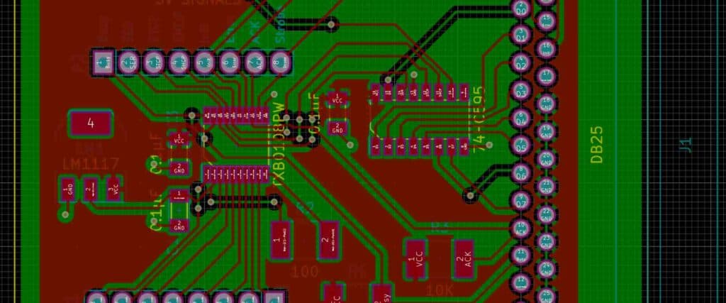
Manufacturing Process for Printed Circuit Boards in IoT
Printed circuit boards (PCBs) are the backbone of IoT devices. The manufacturing process for PCBs involves several stages, including designing, fabrication, assembly, and testing.
Designing
The first step in the manufacturing process is designing the PCB. The design is created using computer-aided design (CAD) software, which generates a schematic of the circuit. The schematic is then converted into a layout, which is a physical representation of the circuit board.
Fabrication
Once the design is complete, the fabrication process begins. The fabrication process involves several steps, including:
- Printing the circuit onto a copper-clad board
- Etching the board to remove unwanted copper
- Drilling holes for components and vias
- Plating the holes with copper
- Applying a solder mask and silkscreen
Assembly
After the fabrication process, the PCB is ready for assembly. The assembly process involves attaching the components to the PCB, which can be done manually or using automated equipment. The components are soldered onto the board using a reflow oven or wave soldering machine.
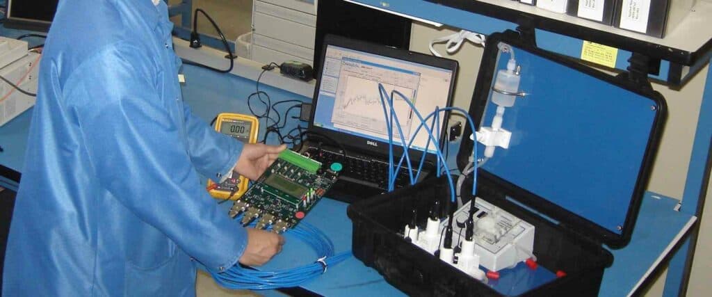
Testing
The final stage in the manufacturing process is testing. The PCB is tested to ensure that it functions correctly. Testing can be done manually or using automated equipment. The PCB is tested for functionality, electrical continuity, and reliability.
In conclusion, the manufacturing process for printed circuit boards in IoT involves several stages, including designing, fabrication, assembly, and testing. Each stage is critical to ensure that the PCB functions correctly.
Quality Control in Manufacturing Printed Circuit Boards in IoT
Quality control is an essential aspect of manufacturing printed circuit boards in IoT. The quality of the circuit boards can significantly affect the performance and reliability of IoT devices. Therefore, it is essential to ensure that the circuit boards meet the required quality standards.
One of the critical quality control measures in manufacturing printed circuit boards is the inspection of the boards. The inspection process involves checking the boards for defects, such as cracks, scratches, and other physical damages. The inspection process also involves checking the boards for electrical defects, such as short circuits and open circuits.
Manufacturers also use automated optical inspection (AOI) systems to inspect the circuit boards. AOI systems use cameras and software to inspect the boards for defects. The AOI systems can detect defects that are not visible to the naked eye, such as soldering defects.
Another critical quality control measure is the testing of the circuit boards. Manufacturers test the circuit boards to ensure that they meet the required specifications. The testing process involves checking the boards for electrical performance, such as voltage, current, and resistance. Manufacturers also test the boards for functionality to ensure that they perform as expected.
In conclusion, quality control is a critical aspect of manufacturing printed circuit boards in IoT. Manufacturers must ensure that the circuit boards meet the required quality standards to ensure the performance and reliability of IoT devices. The inspection and testing of the circuit boards are essential quality control measures that manufacturers use to ensure the quality of the boards.
Future Trends in Manufacturing Printed Circuit Boards in IoT
As the Internet of Things (IoT) continues to grow, the demand for printed circuit boards (PCBs) is increasing. PCBs are the backbone of IoT devices, and their design and manufacturing are critical to the success of IoT products. Here are some future trends in the manufacturing of PCBs for IoT:
Miniaturization
One of the most significant trends in PCB manufacturing is miniaturization. As IoT devices become smaller and more compact, the size of PCBs must also decrease. This trend is driven by the need for smaller and more portable devices. Manufacturers are developing new techniques to create smaller components and reduce the size of PCBs without sacrificing functionality.
Flexible PCBs
Another trend in PCB manufacturing is the use of flexible PCBs. Flexible PCBs are thinner, lighter, and more durable than traditional rigid PCBs. They can bend and twist, making them ideal for use in wearable devices, medical devices, and other applications where flexibility is essential.
Advanced Materials
Manufacturers are also exploring the use of advanced materials in PCB manufacturing. These materials offer improved thermal and electrical properties, making them ideal for high-performance applications. Some of the advanced materials being used in PCB manufacturing include ceramic, metal-core, and flexible substrates.
Automation
Finally, automation is becoming increasingly important in PCB manufacturing. Automation can help reduce costs, improve efficiency, and increase production speed. Manufacturers are investing in automated equipment and software to streamline the manufacturing process and improve product quality.
In conclusion, the future of PCB manufacturing in IoT is exciting. Miniaturization, flexible PCBs, advanced materials, and automation are just a few of the trends that are shaping the industry. As IoT devices continue to evolve, manufacturers will need to adapt and innovate to keep up with the demands of the market.
