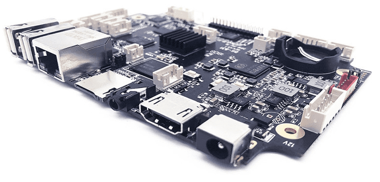
Technological advancements have paved the path for devices to become more efficient and portable. Due to a smaller size, these devices work with circuits of their size too.
Every circuit board is unique and must have the capacity to render different attributes to the gadgets. There is a specific room given to the circuits during the assembly. Smaller circuit boards are commonly to use in different sectors of the world.
There have been several attempts that have induced several properties to these printed circuit boards for many years. The demands for the production and assembly of printed circuit boards vary from one circuit to the other. The prototypes must be capable of meeting all the demands of the users. The performance cannot be compromised.
In this post, we are going to discuss several aspects linked to mini-printed circuit boards in detail.
Applications Of Mini PCB
The size of the developed circuit boards directly relates to the corresponding designs. These are either generated from computers or by using special software. These methods help in the fine development of circuit layouts. Due to this reason, the size of these boards can be reduced easily.
In most cases, the gap between two electrical pathways is always smaller. The circuit’s structure determines the dimensions of printed circuit boards. Also, there is a frame that holds the constituents of the circuit board.
A professional consultation with the manufacturer will help in the accurate small size as per the client’s requirements. Space and frame are two main factors that determine the exact size of the circuit boards. Small devices only work their best with mini-printed circuit boards. The objects for solder paste or green solder mask with mounting holes should be acute and precise to avoid complications. Apply solder paste as per instructions.
Amazing Benefits Of Mini Circuit Board design
There are several benefits of mini-printed circuit boards. Owing to their existence, these are expediting the process of miniaturization. Since technology is progressing at a rapid speed, there are now many producers available that are producing mini electronic devices.
It is because these are portable and consume less space also. Therefore, the presence of small circuit boards becomes crucial for the production of mini gadgets on a commercial scale. Let’s discuss the different benefits of these circuits down below!

1. Room saving PCB design
As discussed earlier, one major factor is that these circuits are space-efficient. This means these are not bulky and gigantic, which makes them difficult to handle the technicians. Smartphones and other small devices contain these circuits in general cases. These circuit boards are easy to assemble because of the higher degree of feasibility offered by such circuits. Also, mini circuits give more space for other components to securely fit in the electronics.
2. Low cost
The process of miniaturization uses these mini circuits. Due to this, such devices become cost-efficient for customers. The production materials used for their production become affordable. Also, investment in transportation becomes easy for both suppliers and producers. Smaller equipment for production needs easy and affordable transportation. Furthermore, these circuit boards are not hefty to produce in terms of the budget needed for the production. In this way, mini circuits offer multiple benefits to reduce the cost as much as possible.
3. Environmentally friendly electronic products
These are environment friendly as well. The materials needed for their production are not many. So that these few components or materials will not create a negative impact on the environment. Also, the fewer the materials, the lesser redundant wastage will be. These are some serious threats to the industry due to the negligence of several manufacturers.
4. More Efficient stock
These circuit boards are unmatched in terms of efficiency. The degree of heat dissipation through these printed circuit boards is impressively less. This can also be one major reason for their abundant utilization in the electronics sector. Due to low dissipation, these offer thermal and electrical characteristics to the devices they are used for.
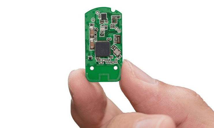
Size of Mini PCB – Reduce the Size of Mini PCB
During the crafting of a mini PCB, it is important to pay heed to its size. It is the only factor that distinguishes these circuits from the others available. It is not wrong to say that experts are conducting many experiments to decrease the size of these circuits and also the size of electronics to provide more ease to users. However, this is not a bigger issue itself. There are 05 common ways to reduce the circuit size and transform it into a mini PCB with the least effort.
· Testing Tools Removal
The removal of testing tools can be helpful in the size reduction of these circuit boards. The former counterparts of such circuits listed pads, headers, and other tools that were designed for debugging and error-removal purposes. These gathered a lot of space, and the size of the circuits could not go any smaller. In the case of size reduction, testing tools like these need secure removal. These days, many circuits don’t need dedicated headers for debugging.
· Multilayer circuit boards usage
Some prototypes only contain one or more layers in the layouts when it comes to circuit designs. These are useful to have an easy reach to the counterparts and traces present in the circuitry. The benefits include inspection, remodification, and repairing as well. After the approval of the layout of mini PCBs, these need an immediate size reduction. Since circuit routing also needs some space for execution. It is important to adjust these components in a careful way to avoid setbacks. This is why multilayer circuits are helpful. These take less space and do their job smoothly.
· Combo Module of Bluetooth wifi
The Bluetooth wifi combo module has its pros and cons in this matter. It includes different modifications related to the circuit boards, wireless connections, and power transformations or conversions. This step is crucial for the design step of the circuits. This can be affordable and expensive, depending on the type of circuit board. The process works with the interlinking of Bluetooth and wifi with a single model with the help of an antenna. Without this, the module fails to function properly as expected.
· Mini PCB and Heavy Copper
In some cases, when we assign a separate large space to these circuits, the traces need a higher degree of current and thermal regulation for precise performance. Due to this, copper is the best solution to reduce the size of the circuit board. Some producers keep the traces as smaller as possible. The weight of a copper layer is not more than 1oz. Adjustments with this copper layer create an impact on the traces as well. The average weight recommended by the experts to develop these circuit boards ranges between 100oz-200oz.
Customization of Length & Width of Mini PCB
Some boards need adjustments to their width and height. If neglected, these can damage the entire structure of the board and might also restrict it from functioning properly. This problem arises when the circuit contains constituents like capacitors, transistors, and headers. When there is no space in the headroom, then the best solution is to keep the wiring at 90 degrees to provide extra room. If it’s something related to capacitors, then dividing the capacitance among smaller counterparts would prove to be helpful in shrinking the size.
· Use of capacitor & resistor
It is important to consider the size of the resistors and capacitors while reducing the overall circuit size. These should always be in small sizes to not compromise the room for the other components. These are special 0805 capacitors that are helpful in this regard. Resistors of the same version are also beneficial. These are much easier to manage. These are dependable to give more space. The package size is also important. This is how the resistors and capacitors are a huge deal in size shrinkage of the circuits if managed properly.
· Shrink the MINI PCB Footprints
Another method is to work on the circuit footprint. It gives a margin to further compress the components and generate more space. These are mechanical layouts for the circuits. 0805 is a typical footprint error. There are different variations possible to execute this. In this case, these variations can exceed the size limit. It is important to have a look at the datasheets to detect any space remaining to position the pads during the design modification. All these measures are viable to decrease the circuit size as per the needs.
Conclusion
The advantages of mini PCBs for consumers are no less. These are an integral part of portable gadgets around the world. These are the backbone of the electronics sector. One helpful technique to reduce the size of the circuit board is to use blind and buried vias. These vias are useful to compress the circuits in size. The production of these circuits is not easy. Due to this reason, the producers have to be vigilant in their manufacturing so that no further complications or mechanical errors will take place on the consumer’s end which would be much harder to address if they prevail.
