PCBs are very important today and are applicable in various areas of the tech world. There are so many types of PCB and by now, you may be wondering what an ultra thin PCB is. Now, this is the case when the thin PCB thickness is more than the standard PCB. The normal thin PCB thickness falls within 1.00 mm and 2.0 mm. The minimum thickness falls within 1L or 2L or 0.3 mm to 0.4 mm. However when the thickness is higher, say about 0.6 mm, then we can name this PCB an ultra thin PCB or long thin PCB.
This article contains everything you are searching for concerning ultra-thin PCB like quality standards, applications, coefficient of thermal expansion, classification, etc. Therefore, if you desire to be a professional in this thin PCB, please continue reading.
Ultra Thin PCB – What is this?
From its name, ultra thin PCB can be referred to as one having a thin pcb thickness compared to the standard type. Also, it is more compact and lighter. This is because the volume of its copper features and its board materials has decreased.
Ultra thin PCB works great for any PCB application where high reliability and miniaturization plays a major role. It helps miniaturization come easy and smoothly with great and enhanced performance via PCB designs with higher density.
Types of Ultra Thin PCBs
Long thin PCB exists in two major types. These are rigid ultra-thin PCB and ultra-thin flexible PCB.
Rigid ultra-thin PCB
Available, are rigid ultra-thin PCB materials that work for applications that require a 2D PCB. Usually, you can apply them as a packaging substrate for ICs – Integrated Circuits. Here they help in transforming the entire component into something very thin.
Here, you can get 25 microns lines or wide spaces, pitches less than 175 microns, and diameters of 100 and 50 microns for the pads and vias respectively.
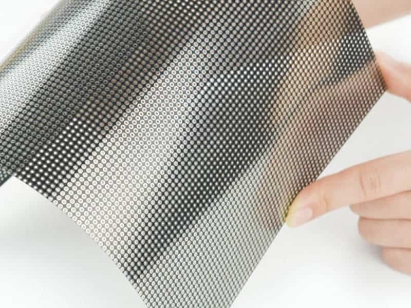
Ultra-thin flexible PCB
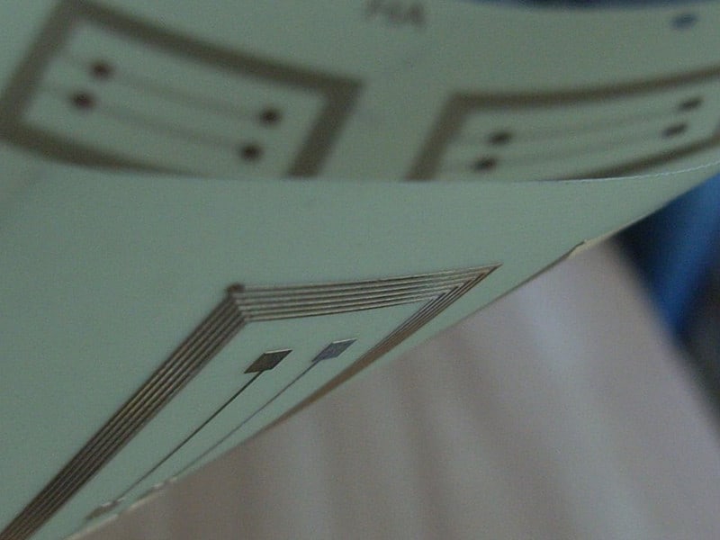
This can also be called ultra thin flex PCB. This long thin PCB is usually manufactured with the use of flexible laminates. By this, the PCB can fold. This reduces the surface area and volume necessary to house or cover the board. By this, the integration density increases.
Furthermore, ultra thin PCB also makes better bending come easy. One area where you can apply ultra-thin flexible PCBs is in manufacturing cables that require dynamic bending. This is because of their high bending capability.
Single-sided Ultra Thin PCB vs. Double-sided Ultra Thin PCB: What’s the Difference?
The single-sided ultra thin PCB features conductive copper and components that are mounted on one of the board’s edges. On its other surface, it also has conductive wiring. These are the only well-known fabricated kinds of long thin PCB. This is as a result of their basic nature and simplicity.
Some common applications where you can apply single-sided PCBs include printers, radio equipment, camera systems, calculators, and more.
Double-sided ultra thin PCBs on the other hand feature traces of two sides featuring a top and bottom layer. They can easily fit the conductive copper and components on any of the board’s surfaces. This enables the traces to be able to pass over another. What results is a circuitry of high density without the need for soldering.
Since the double-sided ultra thin PCBs are much more sophisticated in comparison with their single-sided counterparts, fabricating them could offer more challenge. However, the benefits of double-sided ultra thin PCBs are much more and surpass its disadvantages greatly.
Double-sided ultra-thin PCBs are one of the most common ultra thin PCB types. This is because they help in the production of boards that are very sophisticated. This is beneficial to applications involving electronics of higher technology as well as PCB uses.
The application of double-sided long thin PCBs can be seen in car dashboards, amplifiers, lighting systems, vending machines, and more.
Ultra Thin PCB Applications
You may be wondering where you can use ultra-thin PCBs. Below are some areas where ultra thin PCBs are useful. These include:
- Printers
- Wearable
- Controls for automotive engines
- SIM Card/TF Card
- Metro coins
- Charging modules of mobile phones
- NFC technology device
- GPS system
- Bar code equipment
- Medical devices like hearing aids and active implants
Benefits of Ultra Thin PCB
Long thin PCB comes with some benefits. These include:
Lighter weight
Thinner materials for printed circuit boards leads to smaller lines and spaces, reduced copper plating, reduced aspect ratio of the vias, and smaller vias. This in turn leads to a PCB product that is more lightweight and compact.
Short time for assembly
All the lines of an ultra thin PCB are configured. This saves you some time while connecting excess lines.
Compact and smaller
Long thin PCB has the ability to reduce the end volume of the product effectively. This makes it very portable.
Reduction in Thickness
Ultra thin PCB’s footprint can be minimized considerably when there is miniaturization in both the X and Y axis. However, miniaturization in the Z direction ensures there is additional space for any supplementary component. It also helps in reducing the circuit board’s overall thickness.
Ultra-thin PCB comes with other benefits, which includes good solderability, great heat dissipation, low cost, easy assembly, and more.
The design of ultra thin PCBs helps to compensate for the PCB substrate’s inadequacy regarding the carrying capacity of the component.
To help understand this topic better, let us consider the different types of ultra thin PCBs.
How to Drill Microvias into Ultra-thin PCB
Different techniques exist when drilling microvias into ultra thin printed circuit boards. These include photo-via drilling, plasma etching, and laser drilling. Let’s consider these techniques one after the other.
Photo-via Drilling
Photo-via technology uses lithography patterning and a dielectric material that is photo imaginable. This method has ensured the advancement of the ultra thin HDI PCB. Furthermore, for both the diameter and depth, the size of the hole is about 25 μm. Moreover, this drilling method is expensive due to its dielectric material.
Plasma Etching
This microvia drilling method etches the material of the PCB for hole formation using plasma. Via this technique, you can get a 75 μm diameter for the via home on materials that are 25 μm thick.
However, in addition to costs related to vacuum machinery, this technique is the least when it comes to drilling the via hole.
Laser Drilling
This drilling technology is the most promising of all. Through this technique, you can get the diameter of via hole to 5 μm on dielectric materials having a thickness of 5 μm.
The major factors behind this microvia drilling technique is the wavelength, substrate materials thickness, the substrate material itself and the energy density.
This method is the best for microvias, which has to do with focusing the laser beam on a very small place or area. The cleanliness of the vias that results is just like those obtained via mechanical drilling. This makes sure that depositing plating on the interior of the vias is done uniformly.
This technique comes with a drill speed that is reduced, which contrasts that of mechanical drilling. You can apply this technique to bore the dense microvias effortlessly in an ultra thin PCB, applying any wavelength that spans from ultraviolet to something deep infrared.
Moreover, this technique has a disadvantage. This has to do with its limited depth of laser beam, which you can reproducibly and reliably drill. When you use one lens for the beam concentration, that possible depth the laser can drill becomes limited. This is due to the focus’ depth that has been restricted.
However, a laser beam that is collimated ensures the laser via type of drilling attains a much deeper depth. However, the challenge here is the very small size of the via that leads to the beam’s Fresnel diffraction. In turn, this can impact the intensity of the beam in microvia holes that are exceptionally deep.
Ultra-Thin PCB Standards
Below are some of the quality standards necessary for ultra thin PCB
- ITAR Standards
- ISO Standards
- RoHS Standards
- CE Standards
- REACH Standards
- UL Standards
- IPC Standards
Dielectric Materials Used for Ultra Thin PCB
For long thin PCBs, there are different materials used. For some years now, the standards for the pcb industry has been materials such as polyester and polyimide. Substrates that are epoxy-based, both reinforced and non-reinforced, are used when you consider the cost.
Other materials for PCB like composite, glass, and aramid are useful for some applications that require the main features of performance. To get the best material for your long thin PCB for an application, you have to comprehend the major properties of all materials.
Knowing the thermal mechanical, electrical and chemical characteristics and features of these materials will help you when picking the right base material.
Some mechanical features you should search for are flexibility, tensile strength, strength of tear propagation, and dimensional stability. Also, check for electrical characteristics such as dielectric strength, dielectric constant, and volume resistivity.
You should consider thermal features like temperature of glass transition, range of service temperature, and CTE –coefficient of thermal expansion. However, ensure that you balance the resistance to acids or alkalis and absorption of moisture to meet whatever design characteristics your desire.
What is Impedance Control in Ultra-Thin PCBs?
Impedance control in long thin PCBs involves the coordination of the dimensions and locations of PCB traces to go with your substrate material.
Impedance control ensures that the strength of the signal that travels via a trace doesn’t surpass a specific range. Therefore, it is significant for signals of high frequency travels on the ultra thin PCB’s transmission lines.
To ensure signal integrity, impedance control is very necessary. Since you mount complex processors, antennas, as well as other components directly on the surface of the PCB, there is a surge on the board’s switching of its signal speed.
This ensures that the signal track’s electrical properties are very crucial. This is why the majority of ultra thin PCB design needs impedance control.
Important things to Consider when Constructing Ultra-Thin PCBs
Let us consider some necessary factors you must remember during the construction of ultra-thin pcbs.
Work with a Manufacturer with vast experience
This is very important. Work with a manufacturer having advanced skills in engineering. This is because long thin pcbs require unique design approaches, fabrication technology, and other considerations.
Proper Handling
Proper handling when long thin PCB assembly is on is more important compared to when using ordinary materials. Why this is so is that thinner materials for the substrate may cause greater flexibility and warpage.
The reduced dimensions and smaller pads require higher precision when assembling ultra-thin PCB. However, you may face more challenges when mounting completed circuitry to your board without having to bring damage to them.
This is why it is important to have early discussion with your manufacturer about the amounts of units and handling requirements.
Precise Procedures for Registration
Make use of advanced methods. You must have proper registration processes since when using thinner PCB materials, the features are normally tinier.
Manufacturing Cost
The additional handling and fixtures necessary with the ultra thin PCB materials helps in increasing the assembly and handling costs. However, process and lower material costs can help in balancing all these.
By making use of less copper, you will reduce the materials’ costs. Consulting your engineering team during the design can ensure solutions that are cost-efficient, which satisfies the requirements for your performance.
Conclusion
We hope we’ve been able to cover everything required concerning ultra thin PCB. As mentioned earlier, this type of PCB has a smaller thickness compared to the standard type. It is also more compact and offers less weight. This is due to the reduction in the materials of the board.
Depending on what your unique needs are, RayMing PCB is there to give you the best by offering you custom ultra thin PCBs. You can contact us today to get competitive prices, as well as high performance solutions for your ultra-thin PCB.
