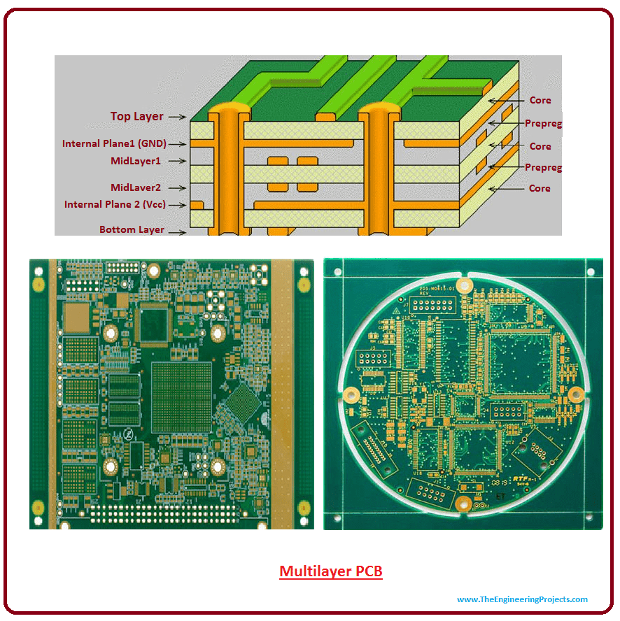
Multilayer PCB fabrication is a multi-stage process. It begins with a design layout and PCB designing software. Then, the layers are stacked, with the inner layer forming the core. Then, we secure the inner layers with either rivets or fusing. Next, we assemble them into the correct order for lamination.
The first step of the multilayer PCB fabrication process is the creation of the inner layer laminate. The inner layers consist of FR-4 material. Then, a layer of copper bonds to the core material. We then cover this layer with a photoresist material. After applying a photoresist layer, we expose the copper thickness to the photoresist. The copper surface is then heated to fuse the layers. In this way, we create a complete circuit board. Finally, we apply the copper to the interior of the drilled holes.
The multilayer PCB is higher quality and more reliable than a single-layer PCB. It is also more robust and requires more insulation between the circuit layers. In addition, it can withstand more weight and heat than a single-layer PCB. In addition, the multilayered PCBs are expensive to produce due to its complexity.
The outer layer of the double sided boards is a fiberglass material that provides the board with core strength. The copper layer is usually a copper foil or full-on copper coating and carries electrical signals.
circuits Stack-Up Design and Lamination Process
Before designing a multilayer PCB stack-up design, it’s essential to understand the different layers and their connections. These are known as the Inner planes, Prepreg, and Coverlay/adhesive layers. The next step in the process is to create a schematic. We can do this by using computer-aided design or other design software. Creating a schematic helps ensure that your PCB design will work. Next, you must determine where to place components and what kind of connection they need.
Inner planes
The inner layer of a multilayer PCB stack-up design and lamination should be symmetrical. This is to avoid potential bow and twist problems. In addition, the designer should monitor PCB emissions during the lamination process. Then, he can minimize PCB emissions and avoid return loops using optimization techniques.
We construct the inner layers of a multilayer PCB design in layers, with the outer layers always made from solid copper foil. These layers provide a path for plating current to flow through the drilled holes. The next layer is typically a prepreg, an epoxy glass cloth coated with epoxy resin. It is then helpful as a glue during the lamination. After assembling the inner planes of a multilayer PCB design, we stack the panels on a heavy metal plate. The stack then moves to a heated hydraulic press.
The inner layers of a multilayer PCB design are crucial for proper signal and power routing. The signal layer should be adjacent to the power and ground layers. They should not be too close or too far apart from each other. The signal layer should be adjacent to the ground layers, with no overlapping layers.
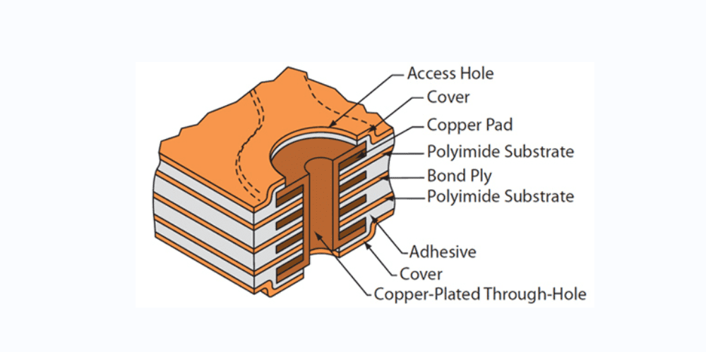
A laminate core separates The inner layers of a multilayer PCB design, the top, and bottom copper layers. The laminate core keeps the layers separate and provides connections between the layers. Vias, meanwhile, provide connections between the two sides of the board.
The multilayer PCB design and lamination are essential for the successful production of electronic circuits. The layer stackup requires the placement of copper layers and insulation layers. In addition, the multiple lamination increases manufacturing costs.
Prepreg
Prepreg is a material used to bond a multilayer PCB design. The process involves alternating layers of different materials in a single PCB unit, ensuring uniform encapsulation of the conductors. The general layers in a PCB stackup design are the PCB cores, glass-reinforced epoxy laminate sheets with copper traces, and the prepregs.
The core is the first layer in a multilayer PCB design, made from more than two layers of copper foil. First, Prepreg is applied to the core’s two copper sides, allowing both buried and blind vias to form.
Using the correct PCB substrate is crucial to the product’s overall performance. An improperly constructed PCB substrate can increase crosstalk, cause interference, and reduce signal integrity. The proper substrate is also critical to the manufacturability of the product. The right substrate will give the double sided PCB a low-inductance power distribution network, which increases the overall product performance.
There are several different approaches to multilayer PCB design. Prepreg is one of the most popular and cost-effective options available. It allows for more flexibility when using multiple layers. A six-layer board will improve EMI dramatically. However, you’ll still have to compromise between trace impedance and desired board thickness.
Choosing the proper material for your double sided PCB core and Prepreg is essential when creating multilayer printed circuit boards stack-up design. Different layers have different dielectric constants, which can cause a significant problem with impedance matching. In addition, different prepreg and core materials have different electrical properties, which can result in impedance-matching issues.
Coverlay/adhesive
There are several factors to consider when choosing a multilayer PCB design. This includes the type of lamination process. There are three lamination processes: sequential, build-up, and cap lamination. Each of them requires different processes and additional time. For example, sequential lamination requires filling vias after each sequential layer, increasing both the cost and delivery time.
First, we should determine the core board thickness by the thickness requirements of the multilayer board. Ideally, the thickness should be uniform, and any deviations should be minimal. Additionally, the distance between the core board and the effective unit must be consistent. Finally, the distance between the effective unit and the board’s edge should also not move. This allows for better space and minimizes material waste.
The next step is to determine the layer count. multilayer printed circuit boards stack-up designs are most efficient when more than two layers exist. A single-sided PCB will not allow for these conductive layers. In addition, because they are thicker than single-sided boards, double sided pcbs require more extensive production processes and planning. However, they are typically higher quality than single-sided boards.
When designing a multilayer PCB, a careful balance between the impedance of the layers is essential. For example, a four-layer board will produce 15 dB less radiation than a two-layer board. Ideally, signal layers will be close together. Quality multilayer PCB design software will help with this process and guide you in selecting suitable materials and impedance levels.
The most common way to manufacture a multilayer PCB is by foil lamination. This is the cheapest and most common method, but there are other methods. The best method to choose depends on your application and budget. For example, you might consider cap lamination when placing a rigid PCBs between the layers.
Glass transition temperature
PCB stack-up design optimization is an integral part of a PCB manufacturing process. In addition, many critical systems’ materials and lamination techniques can dramatically affect how well PCB functions. For this reason, it is essential to understand the different layers and how they influence PCB performance.
The maximum displacement on a CTE curve is the “glass transition temperature” (Td). When this temperature is optimum, the substrate softens and prevents further expansion. In addition, the temperature at which glass transition occurs depends on the material’s thermal conductivity. Low thermal conductivity means that less heat moves. Conversely, high thermal conductivity means that higher heat transfer is possible. We usually measure the heat transfer rate in watts per meter per degree Celsius.
The next step in PCB stack-up design is the lamination process. This step requires a blueprint, which guides the manufacturing process and establishes the materials used for the assembly. Again, having a Bill of Materials (BOM) will enable you to plan materials accurately and choose the appropriate machines.
The glass transition temperature is a critical component of the PCB design process. This temperature determines how much heat a circuit board can withstand before it breaks. This temperature is critical because it affects the connection quality and electrical properties of a PCB. As the PCB gets heated, it is subject to melting and softening, which can lead to connection issues.
A multilayer PCB manufacturing should have a symmetric stack up and core/prepreg thickness. A multilayer PCB with a symmetrical design is critical because the core/prepreg thickness must be the same for each layer. In addition, the design should avoid mixing different layers, as this will cause deformation. A high-frequency laminate made with FR-4 is a good choice for improving impedance values.
Advantages of manufacturing Multilayer PCBs Over Single Layer Alternatives
Multilayer PCBs are a superior option for several reasons. They are reliable and efficient and can accommodate more electronic components. These multilayer pcb advantages make multilayer boards popular for high-speed circuits, which are increasingly becoming a priority in military applications. Furthermore, multilayer boards are smaller than their single-layer counterparts, allowing more room for other components.
Higher reliability
Multilayered PCBs are better than single connection point PCBs for a variety of reasons. Their multiple layers increase their overall reliability, and they can handle more stress and pressure. A multilayer board comprises many thin conductive layers that bond with a prepreg bonding agent. It also provides better protection against heat and shock.
Multilayer PCBs are growing in popularity due to changing trends in the electronics industry. Because of this, many industries have begun using them in their products. For example, many cell phones, modern x-ray equipment, GPS technology, and other high-functioning electronic devices have multilayered PCBs. However, double layered PCBs are expensive and labor-intensive than single-layer alternatives.
Increased efficiency
Multilayer PCBs offer several advantages over traditional PCBs. One of these is the reduction in the size of a product, especially if it is a power-intensive device. Other benefits multilayer PCBs are increased efficiency and reduced EMI shielding. Furthermore, multilayer PCBs are typically more durable. Lastly, multilayer PCBs allow the creation of complex electronic circuits on a smaller PCB. double layered PCBs may cost more, but they are worth it in terms of performance.
Multilayer PCBs have many benefits. They can be helpful in all electronic devices, from simple household appliances to highly sophisticated commercial gadgets. Additionally, multilayer PCBs are thinner and lighter than conventional single connection point PCBs, which is an essential feature for high-tech electronic devices.
Lighter
Multilayer PCBs consist of several layers, increasing the circuitry’s density. The resulting PCBs are lighter and more reliable than single-layer PCBs. Moreover, multilayer PCBs are smaller than single-layer PCBs and are easier to transport.
Multilayer PCBs are extra compact and high-speed, making them ideal for high-frequency devices. In addition, their light weight and compactness make them suitable for mobile devices and high-function electronic devices. As these circuits are becoming increasingly complex, multilayer PCBs are the only way to keep them lightweight.
Ability to accommodate more electronic components
Multilayer PCBs consist of multiple layers of conductive materials. This design allows more electronic components to be on one PCB. Multilayer PCBs are also stronger and more durable than single-layer PCBs. These features make multilayer PCBs an excellent option for several electronic applications.
Multilayer PCBs are becoming more popular with manufacturers. This type of printed circuit board has many advantages and is helpful for mobile electronics. The growth of smart devices, including smartphones, has led to a growing demand for multilayer PCBs.
The major advantage of multilayer PCBs is their ability to accommodate more electronic components. In addition, these boards have a larger area than single-layer PCBs. The underlying substrate can minimize common-mode radiation and minimize EMI. It also reduces crosstalk between traces.
Increased quality
We see Multilayer PCBs as more flexible and allow for more electronic components. They can have anywhere from four to twelve layers. For example, a smartphone will use up to eight layers, while a computer needs up to twelve. Designers generally opt for an even number of layers instead of an odd one, as an odd number can result in a more complicated circuit design and higher costs.
Multilayer PCBs also offer greater design functionality and have better EMI shielding. These rigid flex boards are more expensive to produce, but they offer many benefits. The cost is higher, and you need more advanced tools to produce multilayer pcbs. They also tend to offer increased circuit density and greater operating capacity.
Multilayer PCB Disadvantages
Multilayer PCBs are extra complicated to manufacture than single-layer PCBs. As a result, they are extra expensive. Additionally, multilayer PCBs have more design and fabrication steps, which add time to the production process. However, people who require high-quality, high-capacity electronics are willing to pay more for the added complexity. Furthermore, as technology advances and new production techniques become available, multilayer PCBs will become more affordable to manufacturers.

A disadvantage of multilayer PCBs is that they require a larger design time than single-sided PCBs. In addition, the process is time-consuming, so that it could double the cost of the product. Also, It is difficult to produce multilayer pcbs, so there is a higher risk of errors. Despite these disadvantages, multilayer PCBs can be helpful in many applications.
Multilayer PCBs are generally more durable as compared to the single-sided PCBs. This is because multilayer PCBs include multiple insulation layers between circuit layers. These layers are bound together with a bonding agent and protective materials. However, they may not be suitable for every type of electronic device.
Multilayer PCBs can improve the density of electronic components while also saving space. Additionally, they can increase the functionality of an electronic device. In addition, they can reduce weight and improve EMI shielding. Although some drawbacks are associated with multilayer PCBs, they can make a design much more functional and affordable.
Multilayer PCB Applications
We construct a multilayer circuit board using high temperatures and pressure from Prepreg and core materials fused. This process ensures the uniform encapsulation of conductors and eliminates air between the layers. Next, we cover conductors with resin around the corners. An adhesive material is then melted under a nominal temperature to stick the layers together. This material can be epoxy glass, exotic ceramics, or Teflon. After fusing the layers, we must test them for defects or kinks.
Multilayer PCBs are commonly helpful in electronics that operate in industrial environments. They are rugged and can withstand high temperatures and pressure. As a result, they can be ideal in robotics, automated assembly lines, and car manufacturing. They can also be helpful in medical devices. While these devices are generally handheld or portable, multilayer PCBs are also beneficial in large equipment such as MRI machines.

The use of Multilayer PCBs in electronics requires planning and careful design. This is essential for superior electrical performance. A poorly designed Multilayer PCB can degrade performance due to crosstalk and emissions. Likewise, improperly selected materials can lead to increased noise. Planning the design makes the circuitry more robust and less susceptible to external noise.
Multilayer PCBs are increasingly being helpful in consumer electronics. These devices include all kinds of items we use every day. For example, today’s smartphones have as many as eight layers of PCBs, and there are even three or more layers in military electronic equipment. However, these advanced multilayer PCBs are rare and expensive to produce.
