Pads Logic Layout is a software tool used in the design of printed circuit boards (PCBs). It is an essential part of the PCB design process, as it helps to create the physical layout of the circuit board. Pads Logic Layout is used to place components, route traces, and create the physical design of the board.
The design of a PCB is a complex process that involves many steps. Pads Logic Layout is an important tool in this process, as it helps to ensure that the design is accurate and meets the required specifications. It is used to create the physical layout of the board, which includes placing components, routing traces, and creating the necessary connections between them. Pads Logic Layout is also used to check the design for errors and to optimize the layout for performance and manufacturability.
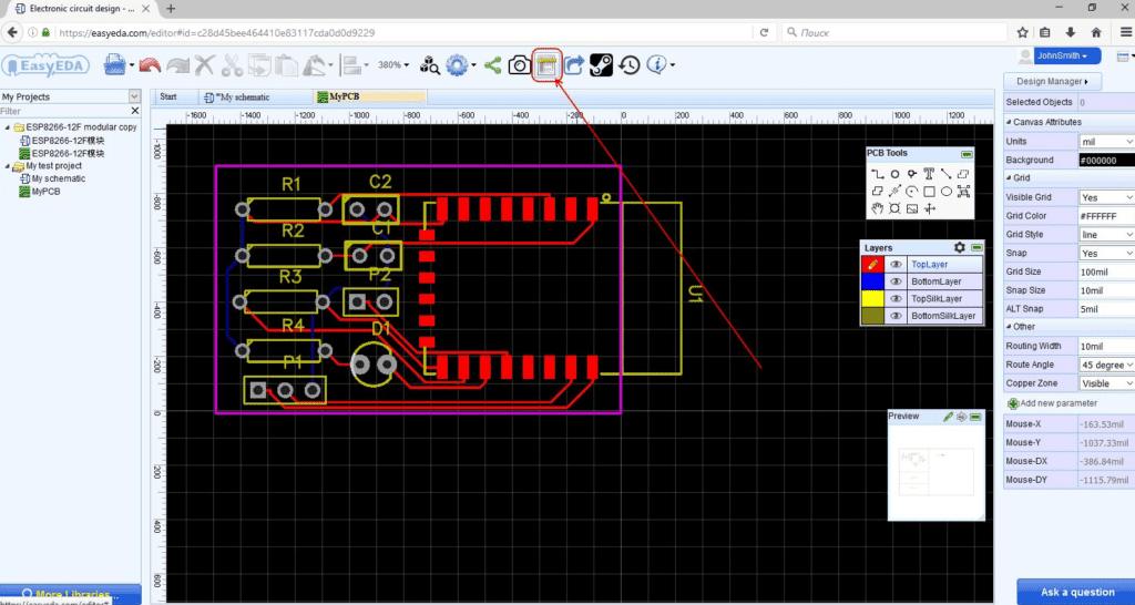
Overview of Pads Logic Layout
Pads Logic Layout is a software tool used to design and layout printed circuit boards (PCBs) for electronic devices. It is a powerful tool that helps engineers and designers create complex PCB designs with ease.
The software provides a user-friendly interface that allows designers to create schematics, place components, and route traces quickly and efficiently. The software also includes a range of features that help designers optimize their designs for performance, reliability, and cost.
One of the key advantages of Pads Logic Layout is its ability to handle large and complex designs. The software can handle designs with hundreds or even thousands of components, making it ideal for use in a wide range of applications.
Another benefit of Pads Logic Layout is its integration with other tools in the Pads suite. This includes tools for simulation, signal integrity analysis, and manufacturing output. This integration helps designers ensure that their designs are optimized for performance and manufacturability.
Overall, Pads Logic Layout is a powerful tool that helps designers create complex PCB designs quickly and efficiently. Its user-friendly interface, powerful features, and integration with other tools in the Pads suite make it an excellent choice for designers looking to optimize their PCB designs for performance, reliability, and cost.
Creating Pads and Traces
Adding Pads
To create a pad in PADS Logic, select the “Add Pad” option from the toolbar or use the shortcut key “P”. Once the pad is added, you can edit its properties such as size, shape, and location. You can also add additional pins to the pad if needed. Pads can be placed on the top or bottom layer of the board, and the software will automatically create vias to connect them if necessary.
Drawing Traces
To draw a trace in PADS Logic, select the “Add Trace” option from the toolbar or use the shortcut key “T”. You can then click on the starting point of the trace and drag it to the ending point. The software will automatically snap the trace to the nearest grid point. You can adjust the width and style of the trace as needed.
When routing traces, it’s important to keep in mind the design rules for your board. These rules will specify the minimum trace width and spacing required for your board’s components and signals. PADS Logic includes a Design Rule Checker (DRC) that will alert you if you violate any of these rules.
In conclusion, creating pads and traces in PADS Logic is a straightforward process that can be accomplished with just a few clicks. By following design rules and using the software’s built-in tools, you can create a professional-looking PCB layout that meets your specifications.
Editing Pads and Traces

Moving Pads and Traces
To move a pad or trace in PADS Logic Layout, follow these steps:
- Select the pad or trace that you want to move.
- Click and hold the left mouse button on the selected pad or trace.
- Drag the pad or trace to the desired location.
- Release the left mouse button to drop the pad or trace in the new location.
Resizing Pads and Traces
To resize a pad or trace in PADS Logic Layout, follow these steps:
- Select the pad or trace that you want to resize.
- Click and hold the left mouse button on the selected pad or trace.
- Drag the mouse to increase or decrease the size of the pad or trace.
- Release the left mouse button to set the new size.
Deleting Pads and Traces
To delete a pad or trace in PADS Logic Layout, follow these steps:
- Select the pad or trace that you want to delete.
- Press the Delete key on your keyboard.
- Confirm the deletion in the pop-up dialog box.
Remember, when editing pads and traces, it’s important to ensure that the layout remains functional and follows design rules. Always double-check your work before saving and moving on to the next step.
Routing and Netlist Generation
Routing Traces
Routing traces is an important part of the pads logic layout process. It involves connecting the various components of the circuit board using traces. The traces are essentially wires that connect the different components of the circuit board. In order to create a good routing layout, it is important to follow certain guidelines. For example, traces should be as short as possible to reduce signal delay and noise. Traces should also be kept away from high-frequency components to reduce electromagnetic interference.
Generating Netlists
Generating netlists is another important part of the pads logic layout process. A netlist is a list of all the connections in the circuit board. It is used to ensure that all the connections are properly made and that there are no errors in the layout. In order to generate a netlist, the circuit board must be properly designed and all the components must be placed in their correct positions. Once this is done, the software will generate a netlist that can be used to verify the layout.
Overall, routing and netlist generation are critical parts of the pads logic layout process. By following the guidelines for routing traces and generating netlists, designers can ensure that their circuit boards are properly designed and will function as intended.
Design Rule Checking

Design Rule Checking (DRC) is a crucial step in the process of designing a Printed Circuit Board (PCB) layout. It ensures that the layout meets the requirements of the manufacturer and the industry standards. DRC verifies the design against a set of rules that define the minimum spacing, trace width, and other parameters that must be followed to ensure the functionality and reliability of the PCB.
DRC is typically performed using software tools that compare the design against a set of rules defined by the manufacturer or the industry standards. The software highlights any violations of the rules and provides suggestions for fixing them. The designer can then modify the design to correct the violations and ensure that the layout meets the requirements.
Some of the common DRC checks include:
- Clearance check: This checks the minimum distance between two objects, such as traces, pads, or vias. It ensures that there is no short circuit or electrical interference between them.
- Width check: This checks the minimum width of a trace. It ensures that the trace can carry the required current without overheating or burning out.
- Hole size check: This checks the minimum and maximum size of a via or a hole. It ensures that the via or the hole can accommodate the required component or the wire.
- Mask check: This checks the minimum distance between a pad and the solder mask. It ensures that the pad is properly covered by the solder mask to prevent short circuits or solder bridging.
In conclusion, DRC is an essential step in the PCB design process. It ensures that the layout meets the requirements of the manufacturer and the industry standards. By using software tools to perform DRC, the designer can identify and correct any violations of the rules and ensure that the layout is functional and reliable.
