PADS PCB Designer is a popular software tool used by electronic engineers to design printed circuit boards (PCBs). It is a powerful and intuitive tool that allows users to create complex PCB designs with ease. PADS PCB Designer is known for its user-friendly interface and advanced features, making it a top choice for both beginners and experienced PCB designers.
PADS PCB Designer offers a wide range of features, including schematic capture, layout design, and library management. The software is designed to be flexible and customizable, allowing users to create their own libraries and templates. PADS PCB Designer also includes a range of built-in tools, such as autorouting and signal integrity analysis, to help users optimize their designs and ensure they meet industry standards.
Overall, PADS PCB Designer is a versatile and reliable tool that is widely used in the electronics industry. Its user-friendly interface and advanced features make it an excellent choice for designing complex PCBs. Whether you are a beginner or an experienced designer, PADS PCB Designer has the tools and features you need to create high-quality PCB designs.
Overview
What is PADS PCB Designer?
PADS PCB Designer is a powerful and intuitive PCB design software that enables engineers and designers to create high-quality printed circuit board designs quickly and efficiently. Developed by Mentor Graphics, PADS PCB Designer offers a comprehensive set of tools and features that help users design complex PCBs with ease.
PADS PCB Designer is a robust and reliable software that is widely used in industries such as aerospace, defense, automotive, medical, and more. It provides users with a complete set of design and analysis tools, including schematic capture, layout, verification, and manufacturing outputs.
Features
PADS PCB Designer offers a wide range of features that make it a popular choice among PCB designers. Some of the key features of PADS PCB Designer include:
-
Schematic Capture: PADS PCB Designer provides an intuitive and easy-to-use schematic capture tool that enables users to quickly create and edit schematics.
-
Layout: PADS PCB Designer offers a powerful and flexible layout tool that enables users to create complex PCB layouts with ease.
-
Design Rule Checking: PADS PCB Designer includes a comprehensive set of design rule checking tools that help users ensure their designs meet industry standards and requirements.
-
Signal Integrity Analysis: PADS PCB Designer includes advanced signal integrity analysis tools that enable users to analyze and optimize their designs for signal integrity.
-
Manufacturing Outputs: PADS PCB Designer provides users with a complete set of manufacturing outputs, including Gerber files, drill files, and bill of materials.
Overall, PADS PCB Designer is a powerful and reliable PCB design software that offers a comprehensive set of tools and features for designing high-quality PCBs. Whether you are an experienced PCB designer or a beginner, PADS PCB Designer can help you create professional-grade PCB designs quickly and efficiently.
System Requirements

Hardware Requirements
To run PADS PCB Designer, your computer must meet the following hardware requirements:
| Requirement | Minimum |
|---|---|
| Processor | Intel or AMD 64-bit processor |
| RAM | 8 GB |
| Hard Disk Space | 10 GB free space |
| Display | 1920×1080 resolution with 16-bit color depth |
| Pointing Device | Mouse or compatible pointing device |
| Network Card | Required for network licensing |
Software Requirements
In addition to the hardware requirements, your computer must also have the following software installed:
- Windows 10 (64-bit)
- Microsoft Internet Explorer 11 or higher
- Microsoft .NET Framework 4.7.2 or higher
- Adobe Acrobat Reader DC or higher
It is important to note that PADS PCB Designer is not compatible with Windows 7 or earlier versions of Windows.
It is also recommended that you have a graphics card with at least 512 MB of dedicated video RAM to ensure optimal performance.
In summary, to run PADS PCB Designer, you will need a 64-bit Windows 10 computer with at least 8 GB of RAM, 10 GB of free hard disk space, and a graphics card with at least 512 MB of dedicated video RAM. You will also need to have Microsoft Internet Explorer 11, Microsoft .NET Framework 4.7.2, and Adobe Acrobat Reader DC installed on your computer.
Installation
Downloading PADS PCB Designer
To install PADS PCB Designer, you first need to download the software from the official website of Mentor Graphics. You can download the software by clicking on the download link provided on the website. The software is available for Windows operating systems only.
Installing PADS PCB Designer
After downloading the software, you can install it by following the installation wizard. The installation wizard will guide you through the installation process step by step. You can choose the installation location and select the components you want to install.
Once the installation is complete, you can launch the software and start using it. The software comes with a user-friendly interface that makes it easy to use.
In conclusion, installing PADS PCB Designer is a straightforward process that can be completed in a few simple steps. With its user-friendly interface and powerful features, PADS PCB Designer is an excellent choice for PCB design.
Getting Started

If you are new to using PADS PCB Designer, this section will guide you through the basics of creating a new project and navigating the user interface.
Creating a New Project
To create a new project in PADS PCB Designer, follow these steps:
- Open the software and click on “File” in the menu bar.
- Select “New” and then “Project” from the drop-down menu.
- In the “New Project” dialog box, enter a name for your project and select a location to save it.
- Choose a project type from the options available, such as “PCB Design” or “Schematic Capture.”
- Click “Create” to create your new project.
Navigating the User Interface
The PADS PCB Designer user interface can be intimidating at first, but it is easy to navigate once you get the hang of it. Here are some tips to help you get started:
- The toolbar at the top of the screen contains all the tools you will need to create your design. Hover over each tool to see a description of what it does.
- The project navigator on the left-hand side of the screen shows all the files and folders in your project. You can expand and collapse folders to view their contents.
- The properties panel on the right-hand side of the screen displays information about the currently selected object, such as its size, location, and properties.
- The main workspace in the center of the screen is where you will create and edit your design. You can zoom in and out using the scroll wheel on your mouse or the zoom slider in the toolbar.
By following these simple steps, you can quickly get started with PADS PCB Designer and begin creating your own PCB designs.
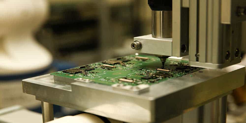
Designing a PCB
Designing a printed circuit board (PCB) can be a complex process, but with PADS PCB Designer, it becomes simpler and more intuitive. This software provides a complete set of tools for designing and verifying a PCB.
Schematic Capture
The first step in designing a PCB is to create a schematic. This is where you define the electrical connections between components. With PADS PCB Designer, you can create a schematic using a wide range of components and symbols. You can also customize the appearance of the schematic to suit your needs.
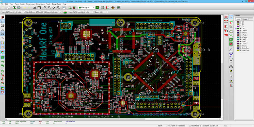
Layout Design
Once you have created your schematic, the next step is to design the layout of the PCB. This is where you place the components and route the connections. PADS PCB Designer provides a powerful set of layout tools that make it easy to create a high-quality PCB layout. You can customize the layout to suit your needs, and the software will automatically check for errors and provide suggestions for improvement.
Design Rule Checking
Design rule checking (DRC) is a critical step in the PCB design process. It ensures that the design meets the required specifications and standards. PADS PCB Designer includes a comprehensive set of DRC tools that automatically check your design against a set of predefined rules. You can also customize the rules to suit your specific requirements.
In conclusion, PADS PCB Designer provides a complete set of tools for designing and verifying a PCB. With its intuitive interface and comprehensive set of features, it makes the PCB design process simpler and more efficient.
Generating Output Files
When you’re finished designing your PCB with PADS PCB Designer, it’s time to generate output files for manufacturing. There are two main types of output files you’ll need: Gerber files and NC drill files.
Gerber Files
Gerber files are the industry standard for PCB manufacturing. They contain all the information needed to create the copper traces, pads, and other features of your PCB. PADS PCB Designer makes it easy to generate Gerber files with just a few clicks.
To generate Gerber files in PADS PCB Designer, follow these steps:
- Click on the “File” menu and select “Export”.
- Choose “Gerber” as the file type.
- Select the layers you want to include in the Gerber files. Typically, you’ll want to include all copper layers, solder mask layers, and silkscreen layers.
- Choose a filename and location for the Gerber files.
- Click “Export” to generate the Gerber files.
NC Drill Files
NC drill files contain the information needed to create the holes in your PCB. PADS PCB Designer can generate NC drill files in a variety of formats, including Excellon and Sieb & Meyer.
To generate NC drill files in PADS PCB Designer, follow these steps:
- Click on the “File” menu and select “Export”.
- Choose “NC Drill” as the file type.
- Select the drill layers you want to include in the NC drill files. Typically, you’ll want to include all drill layers.
- Choose a filename and location for the NC drill files.
- Choose a format for the NC drill files.
- Click “Export” to generate the NC drill files.
That’s it! With just a few clicks, you can generate all the output files you need to manufacture your PCB with PADS PCB Designer.
Advanced Topics
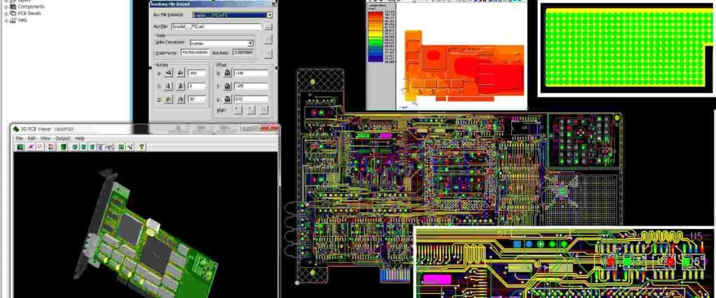
Signal Integrity Analysis
Signal integrity analysis is a crucial step in the design process to ensure that the PCB operates as intended. PADS PCB Designer offers various tools to analyze signal integrity, such as the HyperLynx Signal Integrity tool, which allows designers to simulate and analyze the behavior of signals on the PCB.
The HyperLynx tool provides a range of features, including eye diagrams, impedance analysis, and crosstalk analysis. These features help designers identify potential signal integrity issues and optimize the PCB layout accordingly.
Thermal Analysis
Thermal management is a critical aspect of PCB design, particularly for high-power applications. PADS PCB Designer includes the HyperLynx Thermal tool, which allows designers to simulate and analyze the temperature distribution on the PCB.
The HyperLynx Thermal tool provides various features, such as steady-state and transient analysis, power dissipation analysis, and thermal stress analysis. These features help designers identify potential thermal issues and optimize the PCB layout accordingly.
Overall, PADS PCB Designer offers advanced tools for signal integrity and thermal analysis, allowing designers to optimize the PCB design for performance and reliability.
