PCB assembly used to be a labor-intensive process, but modern technology has made it much faster and more accurate. As a result, machines can work much faster than humans and with fewer components. They also do not get tired easily as humans can. This means faster production times and higher quality products.
Understanding PCB Assembly and Printing
We use PCB assembly and printing processes to produce printed circuit boards. These circuits are generally multi-layered and can vary in complexity. When using advanced electronics, PCB design and construction may become quite complex. Understanding PCB assembly and printing will help optimize your design and manufacturing processes. PCB assembly is the most common way to produce electronic circuits and is an increasingly popular method.
PCB assembly involves placing leads into holes and soldering the components together. This ensures that the components are held firmly in place. In most cases, assembly shops require a minimum space of 10 mm around the board. When assembling, there will also be tests and inspections conducted to ensure the proper assembling of PCB.
To prevent a board from cracking or failing, it is necessary to properly seal and protect the components. There are several types of PCB assembly processes. Typically, the process begins with the design phase. Next, a design review, or DRC, is performed to ensure that the board meets specifications. The DRC ensures that the PCB is in good shape and is free of errors. The design rule check also checks for thin traces and drill hits, which can occur if the bits are dull.
After the design phase, you put the printed PCB together. The printed circuit board has several layers. Each layer gets its printed film. For example, a simple two-layer PCB will require four sheets of film. You then line the films with registration holes on the board, which guide in aligning them properly.
Solder paste printing process

Solder paste is a chemical substance that attaches metal elements to a PCB board. It has many different properties, which determine its viscosity. The higher the metal content in the solder paste, the more viscous the paste will be. Solder paste with thin particles and higher viscosity will result in finer spacing. Solder paste is also a natural material that you can clean with a solvent after soldering.
To print solder paste, you make stencils from polyimide, stainless steel, or paper. The thickness of the stencil determines the solder paste amount you can apply to the PCB. Thinner stencils are good for small components, such as 0603 capacitors and resistors, while thicker stencils are for larger components. For best results, stencils should have an aperture opening at least 10% smaller than the pad size.
Solder paste printing is a complex process. The solder paste is a complex mixture containing small flux vehicle and solder alloy particles. These deposits are critical for a defect-free solder joint, which serves as an electrical and physical connection. As a result, solder paste printing is a reliable, repeatable process that can improve the quality and reliability of PCB assembly.
Solder paste printing is a critical stage of the assembly process, and errors can affect the rest of the process. As such, it is important to have an optimal process to ensure the quality of solder paste. Several factors affect the solder paste printing efficiency, including the temperature, the stencil, and the board itself.
Solder paste printing for PCB assembly requires precise stencil design. Proper stencil design helps ensure the even distribution of solder pastes on your PCB.
FR-4 glass epoxy
When you choose FR-4 glass epoxy for PCB assembly or printing, it is essential to consider the temperature range. Generally, the maximum temperature for a glass epoxy laminate is 300 degrees Celsius, and non-dicy epoxy has a higher limit. FR-4 is commonly used for single-layer PCBs and offers great flexibility for designers and fabricators.
FR-4 glass epoxy is a composite material composed of glass fabric and epoxy resin. You then clad these materials with copper foil and bond them to one or both sides. The result is an extremely rigid and flexible PCB, which is easy to integrate and assemble.
FR-4 PCBs are also available in multilayer and solid core laminates. These laminates offer high stiffness and excellent electrical insulation, which is a crucial characteristic of a PCB. FR-4 also provides excellent fire resistance. If you are in the market for a new PCB for your product, FR-4 may be the best option for your project. Its low-temperature resistance and low flammability make it a great choice for multiple-layer PCBs.
FR-4 glass epoxy is a laminated fiberglass sheet that is fire-retardant. It is a good choice for PCB assembly and printing applications because it is lightweight, strong, and durable. It also possesses high dielectric strength, essential in insulating electronic components and devices.
Always consider the material’s flammability and environmental risks. For example, some epoxy resins can cause allergic reactions and contact dermatitis. They can also be harmful if you breathe their vapor or dust.
Printed circuit board assembly
The assembly and printing of printed circuit boards is a vital process for producing electronic products. Proper quality control is vital to ensure that the finished product is of the highest possible standard. Professional printed circuit board assembly companies use only the best materials and tools when assembling circuit boards. In addition, they ensure that the boards function correctly once fully assembled.
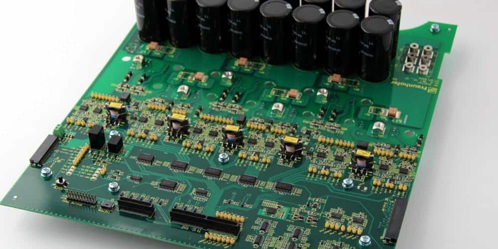
Printed circuit boards have many uses and are in almost any electronic product. They hold a variety of discrete components, ranging from a single-layered board in a garage door opener to 60 layers in a high-speed computer or server. In addition, printed circuit boards are the foundation of other electronic components such as transistors, diodes, and connectors.
To assemble a PCB, you must apply solder paste to the board. A paste stencil is a thin plastic or metal stencil that enables solder paste application to specific parts of the PCB. Using paste stencils can speed up the assembly process. The pick-and-place process is another way to place components on a circuit board.
Before, achieving PCB assembly was through a manual process. Today, this process is automated. Machines can perform tasks faster and with greater accuracy than humans. This helps manufacturers increase their profits. Machines can work efficiently and quickly and they don’t tire easily. Printed circuit board assembly is crucial for electronic devices to operate efficiently and accurately.
The assembly and printing of a PCB is an integral part of the production process, which involves many processes. The process begins with copper foil production on a rigid fiberglass laminate. You selectively etch, drill, and plate this material. The process then continues using chemical baths and silkscreen masks to create the final PCB.
HASL
HASL is a process of coating printed circuit boards in a solder layer. You can use tin or eutectic tin-lead to make the solder. This layer protects the PCB from corrosion and helps attach components to the board. However, many HASL PCBs contain high levels of lead and very harsh flux chemicals, which can be hazardous to human health. Nevertheless, the HASL process does have some advantages.
One of its advantages is the uniformity of the solder coating. However, always use the right amount of flux to achieve an even thickness. In addition, the process requires careful preparation of the copper surfaces. It is also important to control the solder temperature and the length of contact time during the HASL process. Despite these advantages, HASL is not a practical solution for all PCB assembly applications. For example, it is not suitable for fine-pitch components or plated through-holes.
Another benefit of HASL for PCB assembly and printing is its superior surface finish. It can withstand higher levels of oxidation than other PCB Gold surfaces. However, it is still important to properly store your PCBs. The more protection you give your PCB, the less chance of it deteriorating.
HASL is an easy-to-use, inexpensive process. It is comparable to ENIG and offers many benefits. Its low cost and ease of use make it attractive for many PCB assembly and printing applications. However, ENIG is a difficult and time-consuming plating process.
HASL has an excellent wettability and solderability. It can also help to maintain solderability over long periods. The board entry rate and movement away from the solder determines the amount of HASL needed to achieve the desired finish. The angle at which the air knives cut the board and the air pressure is used to apply the solder is also critical to HASL’s appearance.
