PCB design is a complex process that requires careful attention to detail to ensure the final product meets the necessary standards for electromagnetic interference (EMI) and electromagnetic compatibility (EMC) compliance. EMI and EMC are critical considerations for any electronic device, as they can cause interference with other devices, affect performance, and even pose safety risks to users.
EMI refers to the unwanted electromagnetic emissions that can be generated by electronic devices. These emissions can interfere with other devices and cause performance issues. EMC, on the other hand, refers to the ability of an electronic device to function properly in the presence of other electromagnetic emissions. Ensuring that a PCB design is EMI and EMC compliant is essential for ensuring that the final product is safe, reliable, and performs as intended. In this article, we will explore the key considerations for achieving EMI and EMC compliance in PCB design.
PCB Design for EMI/EMC Compliance
When designing a printed circuit board (PCB), it is important to consider electromagnetic interference (EMI) and electromagnetic compatibility (EMC) compliance. EMI refers to the unintentional generation, propagation, and reception of electromagnetic energy that can interfere with the operation of electronic devices, while EMC refers to the ability of electronic devices to operate in their intended electromagnetic environment without causing or suffering from interference.
To ensure EMI/EMC compliance, PCB designers should follow certain guidelines and best practices during the design process. One important consideration is the placement of components on the board. Components that emit high-frequency signals, such as oscillators and clock generators, should be placed away from sensitive components and traces. Additionally, traces that carry high-frequency signals should be kept as short as possible and routed away from sensitive components.
Another important consideration is the use of ground planes and power planes. Ground planes can help reduce EMI by providing a low-impedance path for electromagnetic energy to flow, while power planes can help reduce noise by providing a stable source of power. It is also important to ensure that the ground plane is continuous and that all components are properly grounded.
PCB designers should also consider the use of shielding to reduce EMI. Shielding can take the form of metal enclosures or conductive coatings on the PCB. Additionally, the use of filters and ferrite beads can help reduce EMI by attenuating high-frequency signals.
In summary, designing a PCB for EMI/EMC compliance requires careful consideration of component placement, the use of ground and power planes, and the use of shielding and filtering techniques. By following these guidelines and best practices, PCB designers can ensure that their designs meet EMI/EMC compliance standards and operate reliably in their intended electromagnetic environment.
Key Considerations for PCB Design
When it comes to designing a PCB that meets EMI/EMC compliance, there are several key considerations that must be taken into account. Here are some of the most important factors to keep in mind:
Component Selection
One of the most important aspects of EMI/EMC compliance is selecting the right components for your PCB. This includes capacitors, inductors, and resistors, as well as any other active or passive components that will be used in the design. Make sure that all components are rated for the intended operating conditions and that they are properly grounded and shielded as needed.
PCB Layout
The layout of the PCB is critical for EMI/EMC compliance. The design should be optimized for signal integrity and power distribution, and all traces should be properly routed to minimize EMI emissions and susceptibility. Keep in mind that the placement of components can have a significant impact on EMI/EMC performance, so careful attention should be paid to the placement of sensitive components such as clocks and high-speed data lines.
Grounding and Shielding
Proper grounding and shielding are essential for EMI/EMC compliance. All components should be grounded as needed, and the PCB should be designed with a solid ground plane to provide a low-impedance path for return currents. Shielding can also be used to reduce EMI emissions and susceptibility, particularly for sensitive components such as RF circuits.
Testing and Verification
Finally, it is important to thoroughly test and verify the EMI/EMC performance of the PCB design. This includes both emissions testing (to ensure that the design does not emit excessive EMI) and susceptibility testing (to ensure that the design is not overly sensitive to external EMI sources). Testing should be performed in a controlled environment using appropriate test equipment and procedures.
By keeping these key considerations in mind, you can design a PCB that meets EMI/EMC compliance and performs reliably in its intended application.
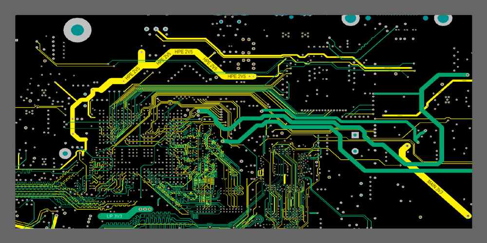
PCB Layout Techniques for EMI/EMC Compliance

PCB layout plays a crucial role in achieving EMI/EMC compliance. Here are some techniques that can help you design a PCB layout that meets EMI/EMC standards:
1. Ground planes
Ground planes are essential for preventing EMI/EMC issues. They provide a low impedance path for return currents and help to reduce ground noise. In addition, they help to reduce the loop area of signal traces, which can help to minimize EMI emissions.
2. Signal routing
Signal routing is another important aspect of PCB layout for EMI/EMC compliance. It is important to keep signal traces as short as possible and to minimize the number of vias and bends. This helps to reduce the loop area of the signal traces, which can help to minimize EMI emissions.
3. Component placement
Component placement is also critical for achieving EMI/EMC compliance. It is important to keep high-speed components away from sensitive components, such as analog circuits. This helps to reduce the coupling between the high-speed signals and sensitive circuits.
4. Shielding
Shielding is another technique that can help to reduce EMI emissions. Shielding can be achieved by using conductive enclosures or shields around sensitive components or circuits.
5. Power and ground filtering
Power and ground filtering can help to reduce EMI emissions and improve EMC immunity. This can be achieved by using decoupling capacitors, ferrite beads, and other filtering components.
By implementing these techniques, you can design a PCB layout that meets EMI/EMC compliance standards.
Grounding and Shielding Techniques
Grounding and shielding are essential techniques to ensure that PCB designs comply with EMI/EMC regulations. Proper grounding and shielding help to prevent electromagnetic interference from affecting the performance of the circuit, and also protect the circuit from external interference.
Grounding Techniques
Grounding involves connecting a circuit to a common reference point, usually the earth. There are several techniques for grounding a PCB design, including:
-
Single-Point Grounding: This technique involves connecting all the ground points in the circuit to a single point, which is then connected to the earth. This technique is useful in reducing ground loops and minimizing the noise in the circuit.
-
Multi-Point Grounding: This technique involves connecting different sections of the circuit to separate ground points, which are then connected to the earth. This technique is useful in reducing the noise generated by high-frequency components.
-
Ground Plane: This technique involves creating a ground plane on one or both sides of the PCB. The ground plane provides a low-impedance path for the return current and helps to reduce the noise in the circuit.
Shielding Techniques
Shielding involves enclosing the circuit in a conductive material to prevent electromagnetic interference from entering or leaving the circuit. There are several techniques for shielding a PCB design, including:
-
Metal Enclosure: This technique involves enclosing the entire circuit in a metal enclosure. The enclosure is connected to the earth to provide a low-impedance path for the EMI/EMC currents. This technique is useful in protecting the circuit from external interference.
-
Shielded Cables: This technique involves using shielded cables to connect the circuit to external components. The shielded cable provides a low-impedance path for the EMI/EMC currents and helps to reduce the noise in the circuit.
-
Ferrite Beads: This technique involves using ferrite beads to suppress high-frequency noise in the circuit. The ferrite bead acts as a low-pass filter and attenuates the high-frequency noise.
In conclusion, proper grounding and shielding techniques are essential to ensure that PCB designs comply with EMI/EMC regulations. By using these techniques, designers can reduce the noise in the circuit and protect it from external interference.
Component Placement and Routing Techniques

Proper component placement and routing techniques are critical to achieving EMI/EMC compliance in PCB design. The following are some guidelines to follow when designing the layout of your PCB:
-
Place components strategically: The placement of components on the PCB can have a significant impact on the EMI/EMC performance of the design. Place components that generate noise, such as switching power supplies and clock circuits, as far away as possible from sensitive components, such as analog circuits and radio frequency (RF) components.
-
Minimize signal loops: Signal loops are a common source of EMI/EMC issues. To minimize signal loops, place components that are part of the same signal path close together and route signals in a direct and efficient manner.
-
Ground planes: Ground planes can help reduce EMI/EMC issues by providing a low-impedance path for return currents. Place ground planes on the opposite side of the PCB from the signal traces and components to minimize interference.
-
Use proper trace routing techniques: Trace routing can have a significant impact on the EMI/EMC performance of the design. Use wide traces for high-speed signals and minimize the length of signal traces to reduce the possibility of signal reflection and crosstalk.
-
Use decoupling capacitors: Decoupling capacitors can help reduce noise on the power supply lines by providing a low-impedance path to ground for high-frequency noise. Place decoupling capacitors as close as possible to the power pins of the components they are decoupling.
By following these guidelines, you can improve the EMI/EMC performance of your PCB design and increase the likelihood of passing regulatory compliance testing.
PCB Stackup Design for EMI/EMC Compliance
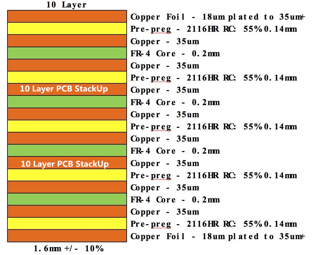
The PCB stackup is an essential part of any electronic device, and its design plays a crucial role in ensuring EMI/EMC compliance. The stackup design determines the number of layers, the thickness of each layer, and the material used for each layer.
One of the most critical aspects of the stackup design is to ensure that the signal and power planes are separated by ground planes. This helps to reduce the coupling between the signal and power planes and minimizes the radiated emissions. The ground planes act as a shield and provide a low-impedance path for the return current.
Another important consideration is the placement of the high-speed signal traces. These traces should be located between the ground planes to reduce the loop area and minimize the radiated emissions. It is also essential to ensure that the signal traces are impedance-controlled to prevent reflections and signal integrity issues.
The thickness and material used for each layer also play a crucial role in EMI/EMC compliance. Thicker copper layers can handle higher currents and provide better shielding. The dielectric material used should have a low dielectric constant and loss tangent to minimize the signal attenuation and reduce the radiated emissions.
In summary, the PCB stackup design is a critical aspect of ensuring EMI/EMC compliance. The stackup should be designed to separate the signal and power planes with ground planes, place high-speed signal traces between ground planes, and use appropriate thickness and material for each layer.
Testing and Verification for EMI/EMC Compliance
After designing a PCB with EMI/EMC considerations in mind, it’s important to test and verify its compliance with relevant standards. This ensures that the product will function properly and not cause interference with other electronic devices.
There are various types of tests that can be performed, including radiated emissions, conducted emissions, radiated immunity, and conducted immunity. Radiated emissions testing involves measuring the electromagnetic radiation emitted from the PCB, while conducted emissions testing measures the amount of electromagnetic interference conducted through the power and signal lines.
Radiated immunity testing evaluates the resistance of the PCB to external electromagnetic radiation, while conducted immunity testing evaluates its resistance to conducted electromagnetic interference. These tests are typically performed using specialized equipment in an anechoic chamber or shielded room.
It’s important to note that testing for EMI/EMC compliance should be done throughout the design process, not just at the end. This allows for any issues to be identified and addressed early on, which can save time and money in the long run.
In addition to testing, it’s also important to verify compliance with relevant standards. These standards vary depending on the industry and application, but common ones include FCC Part 15, CISPR 22, and IEC 61000-4-x. Verification can be done through self-declaration or third-party testing and certification.
Overall, testing and verification for EMI/EMC compliance is a crucial step in the PCB design process. By ensuring compliance with relevant standards, designers can create products that function properly and don’t interfere with other electronic devices.
