The printed circuit board is one of the most crucial parts in an electronic design and a key concept in electronics generally. PCB is so fundamental that people often forget to explain what it is or how to design it the right way.
Meanwhile, electronic devices are a vital part of the modern world, from smartphones with streams of notifications to vitals-monitoring devices. Each electronic device features a printed circuit board at the heart of its design. The difference is that while some come with smaller boards that use a common material and a bottom layer, others come with larger boards.
As the years rolled by, PCB manufacturing has consistently grown to keep up with the growing demand of more complex electronic circuitry, design rules, and component leads. PCBs are present in nearly all electronic circuits and products; they have overtaken point-to-point construction and wire-wrap, which were once popular.
However, PCB design requires additional effort for the circuit layout or drill file, but the good news is that assembly can be automated. In this article, we will explain the concept of printed circuit boards and how to design an electronic circuit from scratch.
Printed Circuit Boards: Understanding the Concept
Printed circuit boards, also known as printed wiring cards or printed wiring boards, are boards with lines and pads connecting various points together. In a PCB, individual traces electrically connect the various components and connectors together, the PCB allowing signal and power routing between physical devices.
There are electrical connections between the electronic components and the surface of the PCB; this is made by solder. Solder is a metal that serves as a strong mechanical adhesive for holding electrical components together.
A PCB is a firm structure of an electrical circuitry composed of large area metal called planes and traces [which are embedded metal surfaces]. They are built with a dielectric core material with poor electrical conductivity, thus ensuring pure circuitry transmission. This also ensures there is interspacing with extra layers of dielectric and metal as required.
How Did PCBs Come About?
Before printed circuit boards came about, circuits were constructed via a laborious point-to-point wiring process. As a result, there were frequent failures, particularly at short circuits and wire junctions when wire insulations age and crack.
Then came wire wrapping, which marked a significant advancement, where a small gauge wire is wrapped around a post at each connection point. This creates a highly durable and easily changeable gas-tight connection.
However, electronics began to evolve from vacuum tubes and relays to integrated circuits and silicon. As things began to change, the size and cost of electronic components started to decrease.
Meanwhile, electronics became more prevalent in consumer goods, leading to a pressure to reduce the manufacturing costs and size of electronic products. In a bid to find better solutions to the problem, manufacturers invented printed circuit boards.
What Is a PCB Composed Of?

A PCB features alternating layers of different materials laminated together with adhesive and heat resulting in a single object. It comprises the FR4, which is the substrate or base material giving the PCB its common thickness and rigidity.
The copper layer, which is a slim copper foil that is laminated to the board using heat and adhesive, comes after. Copper is applied to both substrate sides on common double-sided PCBs; “double-sided” refers to the number of copper layers in the board.
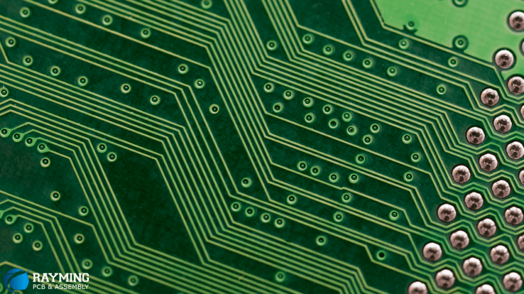
The copper thickness varies from one ounce per square foot to up to three ounces; each ounce is about 35 micrometers. Next, the solder mask layer; this is the top layer of the copper foil, giving the PCB its green or red color. This layer is overlaid onto the copper layer to insulate copper traces, preventing accidental contact with conductive bits, solder, and other metal like aluminum .
Lastly, the white silkscreen; this is located atop the solder mask layer, adding letters, numbers, and symbols to the PCB. This enables easier indicators and assembly for people to better understand the board. These silkscreen labels are often used to indicate each pin’s or LED’s function.
What Categories of Printed Circuit Boards Are There?
There are majorly three categories of printed circuit boards: rigid, flex, and metal-core PCBs. The most common type of board a designer will encounter is the rigid PCB; the board layout is contained within a rigid substrate. These boards are commonly designed with FR-4, although this can be modified depending on the design needs.
Flexible PCBs have less rigid materials, which are tactilely reminiscent of a film roll, allowing for greater deflection. The board thickness of flexible PCBs is less standard than the rigid PCB. However, these boards are expected to usher in the next stage of wearable technology and eliminate planar constraints in rigid board devices.
Metal-core circuit boards are an offshoot of rigid PCB designs but with a higher ability to dissipate heat throughout the board. These types of PCB are the best for high-current designs as they protect sensitive circuitry and prevent thermal wear and failure.
What Are PCBs Used In?
PCBs are used in electronic and electrical engineering to connect one electronic component to another in a controlled manner. The board takes the structure of a laminated sandwich of conductive and insulating layers, each conductive layer designed with traces, planes, and other features.
The electrical components of boards may be fixed to conductive pads on the outer layers; these pads are designed to accept component’s terminals by soldering. Connection and fastening is done both electrically and mechanically.
Otherwise, the components may be fixed through plated-through holes that enable interconnections between layers. PCBs are used in almost all electronic devices and products; they can be made manually in small quantities or automatically in large quantities.
PCB mass production is cheaper and faster as there is electronic design automation software available to do most of the layout work.
How Many Sides Does a PCB Have?
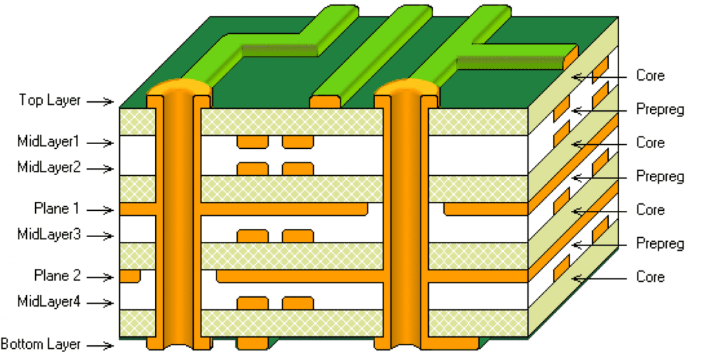
PCBs come in different designs and with a varying number of components: single-sided, double-sided, and multiple layers. A single-sided PCB has one copper layer while the double-sided PCB has two on both sides of one substrate layer.
Multi-layer PCBs, on the other hand, feature outer and inner layers of copper, which alternate with substrate layers. Multi-layer PCBs feature circuit traces on the inner copper layers, thus allowing for a high density interconnect.
There is a rising popularity in the manufacture of multi-layer PCBs, especially those with more than two copper planes. However, while they offer many benefits, multi-layer PCBs also have their demerits. For instance, it is much more difficult and impractical to make analysis, repair, and field modification of circuits.
The Structure of a Basic PCB
A basic PCB features a flat sheet of insulating material and copper foil laminated onto the substrate. The copper is divided through chemical etching into separate conducting lines called circuit traces or tracks, pads, and vias.
The surface mount pads are used for connections while the via passes connections between copper layers. The PCB surface may have a coating protecting the copper from corrosion and reducing the chances of undesired electrical contact with stray bare wires.
The “artwork” is the pattern etched into each copper component, which is usually done using photoresist coated onto the PCB. The material protects the copper from dissolving into the etching solution, and then the etched board is cleaned. A PCB without components installed is less ambiguously referred to as an etched wiring board or printed wiring board (PWB).
What Is the Simplest PCB to Produce?
The two-layer PCB is one of the simplest circuit boards to produce; it features copper on both sides. The copper on both sides are referred to as external layers, with multi-layer boards sandwiching additional internal copper structures and insulation.
Next to the two-layer PCB is the four-layer circuit board; this board adds more PCB routing options in the internal layers than two-layer boards.
More often than not, some parts of the internal layers of four-layer boards are used as power planes or ground planes. This is done to ensure better power supply decoupling, better signal integrity, lower EMI, and higher signaling frequencies.
In multi-layer boards, including four-layer boards, the material layers are laminated together in an alternating sandwich, with each copper plane etched.
Also, internal vias are plated-through before the layers are laminated and only the outer layers require coating. Furthermore, the internal layers are protected by the adjacent traces and substrate layers.
How Are Components Mounted in PCB Layout?
PCB components are mounted through through-hole or surface mount technology; sometimes, a PCB may use both methods for component mounting. In through-hole mounting technology, components are mounted through their wire leads being passed through the board and soldered to traces. In surface mount technology, components are mounted by their leads to copper placements on the board.
In through-hold mounting, the component leads are soldered to traces on the other side of the circuit board. Contrarily, in surface mount components, the leads are soldered to copper traces on the same side of the board with the appropriate solder mask.
Through-hole mounting has grown less common, with surface mounting technology (SMT) being cheaper, faster, and much easier. Where through-hole component mounting is used for large components like connectors and electrolytic capacitors, surface mounting is used for capacitors, transistors, diodes, resistors, and IC chips.
What Are the Electrical Properties of a PCB?
Each trace on a PCB features a flat, narrow portion of the copper foil remaining after etching. Its resistance, which is determined by its length, width, and thickness, must be low for the current the conductor carries.
Meanwhile, there may be a need to differentiate between the traces used for the power and the ground and those used for the signal. For more than one PCB layer, you must ensure a layer is composed primarily of solid copper PCB for the ground plane to ensure power return and shielding.
Best Design Practices for Printed Circuit Boards
If you are giving your circuit design project to a PCB or flex application engineer, clear communication is essential. You want to communicate with the engineer at the beginning of the project, discussing everything you require for it.
With open and constant communication, you and your PCB provider will be on the same page, thus reducing the need for multiple revisions. Although a 100% perfectly-designed PCB is rare on the first try, communication helps ensure you start on good footing.
When you give your PCB engineer the design, ensure you provide the right board size, materials, trace width, component placement, and tolerances. For flexes, you will need to decide whether the design is dynamic, static, or partly flexible.
Also, consider the environment in which you will use the PCB: for a non-extreme environment or a high-extreme environment? Over the next few subheadings, we will discuss the proper way to design a printed circuit board from scratch.
Step 1: Understanding the Electrical Parameters and Creating a Circuit Diagram
Before you start designing your printed circuit board, you need to get a good grasp of the system’s electrical parameters. These parameters may vary from the current maximums to the shielding considerations and capacitance limitations in place. Other parameters may include signal types and voltage to be used.
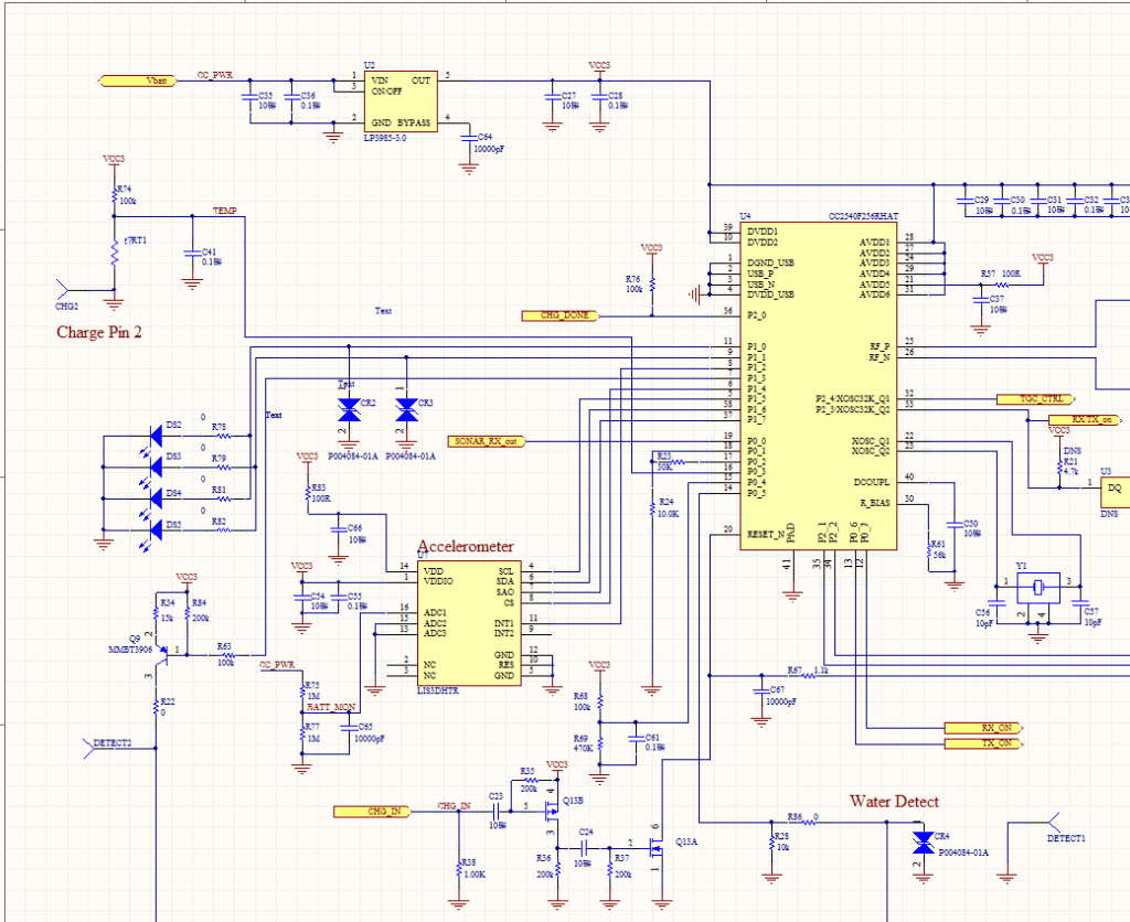
Once you understand the parameters, you need a circuit diagram to determine the type of circuit you want to build. There are two ways to do this: either you draw yours from scratch or find one someone else already made.
Step 2: Drawing Your PCB Schematics
PCB schematic creation means creating logic symbols for the parts you will implement, including the integrated circuits (ICs), resistors, capacitors, metal core boards, molten solder, connectors, hole components, and inductors. This creation is what is referred to as the schematic diagram and is expected to have certain hole components that makes it easy to drill holes in them.
Creating a schematic is one of the first steps in PCB design basics; it defines the board’s purpose and function at the electrical level and provides for certain specifications like the drill holes. When you have a diagram in place, it becomes easy to understand PCB design basics and work through hole components provided for the manufacturing process.
You will need to install a PCB design software tool for this. When the parts are ready for use, you can start organizing them roughly on schematic sheets within the CAD tools on the PC board. When doing so, pay attention to every item of the CAD tools, including the epoxy ink.
When you have roughly placed them, you can draw wires to represent the connectivity between the pins of the schematic symbols. The lines or nets can represent single nets or groups for memory or data circuits. You will need to move process parts as needed during the schematic capture to create a legible and clear schematic.
Step 3: Simulating the Circuitry
Once the nets and parts have been organized on the schematic, the next step is to verify that the circuit will work as intended. To do this, use circuit simulations with SPICE, the Integrated Circuit Emphasis tool, in a simulation program on the gerber files. PCB engineers use these tools to test the two circuit boards they are designing before they go ahead to build the actual hardware.
These tools are a vital part of the PCB design process, especially because they help PCB engineers save time and money. Creating a PCB layout will show you exactly where your components will be placed and how the board will operate.
Step 4: Set Up Your CAD Tool and Layout Components
The PCB design tools used by PCB engineers are able to set up design rules and constraints to prevent issues of overlapping with distinct nets. At the same time, they help ensure that the appropriate distance between different objects is maintained. Design grids, for instance, helps a designer place components and route traces neatly and orderly.
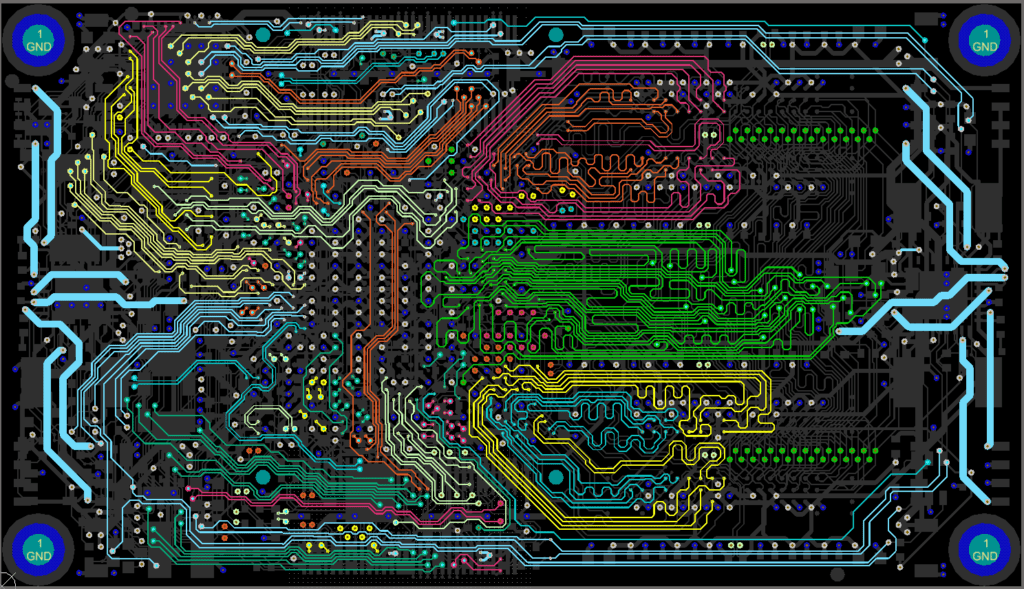
After setting up your design database and net connectivity information imported from the PCB schematic. The next task is the physical layout of the circuit board.
First, place the component footprints in the CAD system within the board outline; each has the net connections displayed as ghost-line images. Place these parts while staying mindful of connectivity, excessive heat, electrical noise, and other physical obstructions like cables and connectors.
Step 5: Routing the Printed Circuit Board
The components have been correctly placed (you can move these if the need arises); the next thing is net connection. To connect the nets together, convert the rubber net connections into drawn planes and traces; the CAD tools enable this. You need to be careful when routing, ensuring the nets are the right length for the signals they will be conducting.
Also, great care must be taken to ensure the nets do not cross areas of excessive noise. If this happens, there can be signal integrity problems such as cross-talk, which may degrade the performance of the newly-built PCB.
Step 6: Ensuring a Clear Return Current Path
The ICs and other related active components on the PCB need to be connected to ground and power nets. You can easily do this by flooding layers or areas with solid planes that the components can tap into. However, this is easier said than done as these planes are also responsible for returning the signals routed with traces.
If there are too many holes, splits, or cut-outs in the planes, the return paths can create a lot of noise. As a result, the performance of the newly-designed printed circuit board will be degraded.
Step 7: Run a Final Rules Check
Now that you’re done with the power and ground planes, component placement, and trace routing, your PCB layout is almost ready. Before you begin the actual designing, you want to run a final rules check on it. This is where you will set up the different markings and texts that will be silk-screened on the board’s exterior.
The markings enable others to find the components and label the board with names, copyright information, and dates. Also, you will need to output drawings that will be used in manufacturing for the final PCB fabrication and assembly.
Step 8: Build Your Board
Now, you are all set to start building the board, starting with sending the output data files to a facility like Hillmancurtis for fabrication. The fabrication process covers etching all the traces and planes onto the different metal layers and compressing them in one. The result is a bare board ready for assembly, which the assembly facility will load with the needed components.
The board will then be run through different soldering processes, depending on the type of components you are using. When the actual board design is done, it is inspected and tested before the final product is shipped to you.
Why Should You Choose Hillmancurtis?
Hillmancurtis is a PCB manufacturing and assembly company that offers high-quality PCB fabrication, PCB assembly, and components sourcing. The company has more than ten years of experience in the industry of electronics manufacturing.
The company’s mission is to provide high-quality PCB manufacturing and assembly services that surpass its clientele’s expectations and at economical prices. More so, it operates and complies with laws, regulations, and rules, acting with the highest ethical standards and good social conscience.
As you may have guessed, the process of PCB fabrication and assembly are demanding and must be exact. If you want a circuitry that delivers the required performance, PCB manufacturers need precise data to work with. Only a company that has the functionality and features required for creating complex designs such as Hillmancurtis can ensure this.
Conclusion
PCB layout design typically features a polyimide-based or copper-clad film for flex circuits and FR4 stiffener for rigid-flex. Also, a solder mask is required for coating everything on the board with a cover coat or epoxy resin LPI.
Summarily, to design your own PCB layout from scratch, you need to first find a CAD package. To choose the best, consider the community support, ease of use, capability, and portability of the package. Also, don’t overlook schematics and maintain low, realistic expectations; as this is your first, expect a lot of problems.
