Table of Contents
ToggleA full wave rectifier is an electronic circuit that converts an alternating current (AC) to a direct current (DC). It is commonly used in power supplies and electronic devices that require a steady and reliable DC voltage. PCB design plays a crucial role in the performance and efficiency of a full wave rectifier.
The PCB layout for a full wave rectifier should be designed to minimize noise and interference, reduce heat dissipation, and ensure proper voltage regulation. The placement and routing of components, such as diodes, capacitors, and resistors, should be carefully planned to optimize the circuit’s performance. Additionally, the size and thickness of the copper traces and the choice of materials for the PCB can affect the rectifier’s efficiency and reliability. In this article, we will explore the important considerations and best practices for designing a PCB for a full wave rectifier.

PCB Design for Full Wave Rectifier
Schematic Design
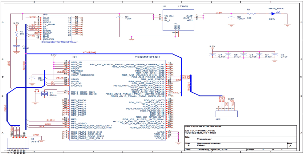
Before starting the PCB design for a full wave rectifier, it is essential to create a schematic diagram. The schematic diagram will help in identifying the components required for the circuit and their interconnections. It is important to ensure that the schematic diagram is accurate and complete before proceeding to the next step.
Component Selection
The selection of components plays a crucial role in the performance of the full wave rectifier circuit. The diodes used in the circuit must have a high current rating and low forward voltage drop. The capacitors used in the circuit must have a high voltage rating and low ESR. It is recommended to use surface mount components to reduce the size of the PCB.
Layout Design
The layout design is the process of placing the components on the PCB and routing the traces to connect them. The layout must be optimized for signal integrity, thermal management, and manufacturability. It is recommended to follow the manufacturer’s guidelines for the placement of components and the routing of traces.
Routing
The routing process involves connecting the components using traces on the PCB. The traces must be designed to carry the required current without causing voltage drops. It is recommended to use wide traces for high current paths. The traces must also be designed to minimize electromagnetic interference (EMI) and crosstalk.
Testing and Troubleshooting
After the PCB is manufactured, it is essential to test the full wave rectifier circuit for proper functionality. The testing process involves measuring the output voltage and current of the circuit under different load conditions. If any issues are identified, it is recommended to troubleshoot the circuit by checking the connections, component values, and PCB layout.
In summary, the PCB design for a full wave rectifier requires careful consideration of the schematic design, component selection, layout design, routing, testing, and troubleshooting. By following the best practices and guidelines, it is possible to design a reliable and efficient full wave rectifier circuit.
Schematic Design

Circuit Diagram
The first step in designing a full wave rectifier PCB is to create a circuit diagram. The circuit diagram should include all the necessary components such as diodes, resistors, and capacitors. It should also show the connections between the components and the input and output terminals.
When creating the circuit diagram, it’s important to keep in mind the voltage and current requirements of the circuit. The diodes used in the rectifier must be able to handle the maximum voltage and current that will be passed through them.
Component Placement
Once the circuit diagram is complete, the next step is to place the components on the PCB. The placement of components is important for the overall performance of the circuit. Components that are placed too close together can cause interference and noise. Components that are placed too far apart can cause signal loss.
When placing components on the PCB, it’s important to consider the size and shape of each component. Components that are larger or have odd shapes may need to be placed in specific locations to avoid interference with other components.
In addition to component placement, it’s also important to consider the routing of the traces on the PCB. The traces should be routed in a way that minimizes interference and noise. They should also be routed in a way that minimizes signal loss.
Overall, the schematic design of a full wave rectifier PCB is critical to the overall performance of the circuit. By carefully designing the circuit diagram and placing the components correctly, you can ensure that the circuit will function properly and reliably.
Component Selection

When designing a full wave rectifier, selecting the right components is crucial to ensure a smooth and efficient operation. The three main components to consider are diodes, capacitors, and resistors.
Diodes
Diodes are essential components in a full wave rectifier circuit. They allow current to flow in only one direction, which is crucial for rectifying AC voltage. When selecting diodes, it is important to consider their forward voltage drop, reverse voltage rating, and maximum current rating.
For a full wave rectifier, Schottky diodes are often a good choice due to their low forward voltage drop and fast switching speed. However, they have a lower reverse voltage rating compared to other diodes, so it is important to select a diode with a reverse voltage rating that exceeds the maximum expected reverse voltage.
Capacitors
Capacitors are used in full wave rectifiers to smooth out the rectified output voltage. When selecting capacitors, it is important to consider their capacitance value, voltage rating, and equivalent series resistance (ESR).
Electrolytic capacitors are commonly used in full wave rectifiers due to their high capacitance values and relatively low cost. However, they have a limited lifetime and may fail if subjected to high temperatures or voltage spikes. It is important to select a capacitor with a voltage rating that exceeds the maximum expected voltage and to consider the ESR, which can affect the ripple voltage.
Resistors
Resistors are used in full wave rectifiers to limit the current flowing through the diodes and to provide a load for the rectified output voltage. When selecting resistors, it is important to consider their resistance value, power rating, and tolerance.
For current limiting resistors, it is important to select a resistor with a power rating that exceeds the maximum expected power dissipation and to ensure that the resistance value is appropriate for the expected current. For load resistors, the resistance value should be selected based on the desired output voltage and current, and the power rating should exceed the maximum expected power dissipation.
Overall, selecting the right components is essential for designing a reliable and efficient full wave rectifier circuit. By considering the specifications of diodes, capacitors, and resistors, designers can ensure that their circuit will function correctly and provide the desired output voltage.
Layout Design

PCB Size and Shape
The size and shape of the PCB are important considerations when designing the layout for a full wave rectifier. The PCB should be large enough to accommodate all the required components and provide sufficient space for routing the traces. The shape of the PCB should also be considered, as it can affect the overall performance of the circuit. For example, a rectangular PCB may be more suitable for circuits that require a linear flow of current, while a circular PCB may be more suitable for circuits that require a circular flow of current.
Placement of Components
The placement of components is critical for the proper functioning of the full wave rectifier. The components should be placed in a way that minimizes the length of the traces and reduces the possibility of interference between components. The diodes should be placed close to the transformer, and the filter capacitors should be placed as close as possible to the rectifier output. The placement of the transformer should also be considered, as it can affect the overall performance of the circuit.
Grounding
The grounding of the PCB is crucial for the proper functioning of the full wave rectifier. The ground plane should be designed in a way that minimizes the length of the traces and reduces the possibility of interference between components. The ground plane should be connected to the circuit ground at a single point, and the ground plane should be kept away from the signal traces. The ground plane should also be designed in a way that minimizes the possibility of ground loops.
Power Planes
The power planes are essential for the proper functioning of the full wave rectifier. The power planes should be designed in a way that minimizes the length of the traces and reduces the possibility of interference between components. The power planes should be connected to the power supply at a single point, and the power planes should be kept away from the signal traces. The power planes should also be designed in a way that minimizes the possibility of ground loops.
In summary, the layout design for a full wave rectifier is critical for the proper functioning of the circuit. The PCB size and shape, placement of components, grounding, and power planes should be carefully considered to ensure the best possible performance of the circuit.
Routing

When routing a full wave rectifier PCB, there are several important considerations to keep in mind. In this section, we will discuss trace width and spacing, signal integrity considerations, and via placement.
Trace Width and Spacing
The trace width and spacing of a PCB can have a significant impact on its performance. For a full wave rectifier, it is important to ensure that the traces are wide enough to handle the current and that there is enough spacing between them to prevent any unwanted coupling.
The table below provides some general guidelines for trace width and spacing based on the current being carried:
| Current | Trace Width | Spacing |
|---|---|---|
| 1A | 20 mils | 20 mils |
| 5A | 40 mils | 40 mils |
| 10A | 60 mils | 60 mils |
Signal Integrity Considerations
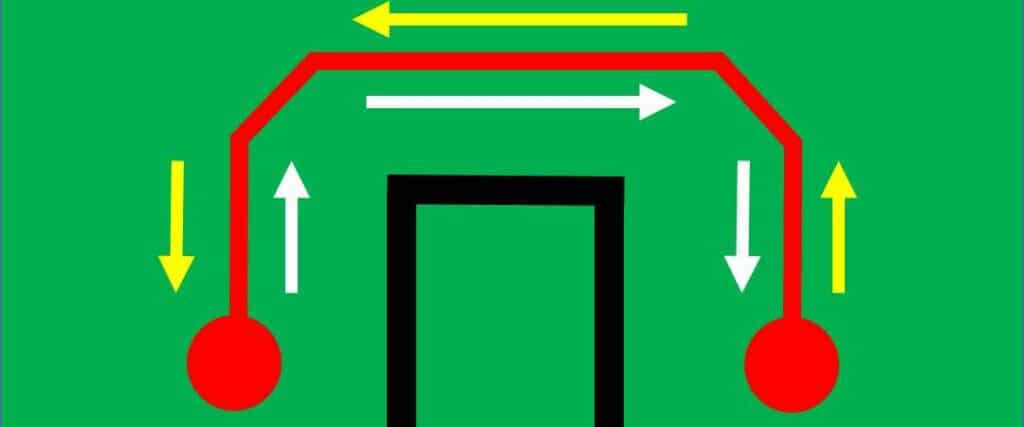
Signal integrity is critical for any PCB design, and a full wave rectifier is no exception. When routing the PCB, it is important to minimize the length of the traces and to avoid any sharp turns or corners.
In addition, it is important to ensure that the ground plane is properly connected and that there is adequate shielding to prevent any interference from external sources.
Via Placement
Vias are an important part of any PCB design, and their placement can have a significant impact on the performance of the circuit. When routing a full wave rectifier, it is important to ensure that the vias are placed in a way that minimizes their impact on the signal integrity of the circuit.
One common approach is to place the vias near the pads of the components, as this helps to minimize the length of the traces and reduce any unwanted coupling.
In summary, when routing a full wave rectifier PCB, it is important to consider trace width and spacing, signal integrity considerations, and via placement. By keeping these factors in mind and following best practices, you can ensure that your design performs as intended.

