Four (4) major steps are used when making a Printed Circuit Board (PCB). Overlooking one of these steps could make a lot of difference in how the board eventually turns out to work. This is the reason why most manufacturers hit hard on using PCB fabrication services.
In this article, we extensively talk about the meaning of circuit board fabrication, why it is important and some of the differences between it and circuit board assembly.
What is PCB Fabrication?
It is a process by which is a Printed Circuit Board (PCB)’s design is transferred to the circuit board ahead of the design.
Without the design, the project wouldn’t go on, considering that the design shows the processes to be taken. By transferring the design to the bare board, it becomes easier to view the different points and places that the components need to be attached.
The Relationship between PCB Fabrication & Other Circuit Board Development Stages
You can consider the transfer of the design to the bare board as the second step in the development iteration.
Here is a summary of the different stages that go into the development of PCBs:
Board Design
This has to do with designing or making the early-stage schematics of how the PCB would function. It is the design that helps in mapping the components.
Once the board’s design is ready, it can then be transferred to the bare board. That is the second stage – fabrication.
Circuit Board Fabrication
Here, the readied design will be creating the design on a bare board, which doubles as the foundation of the Printed Circuit Board (PCB).
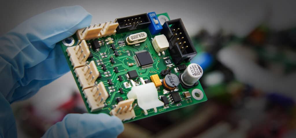
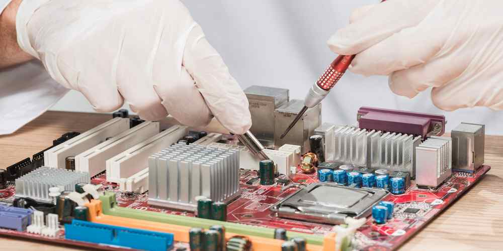
PCBA
When the bare board is created, it would be time to start placing or assembling the parts/components on it. This is what is known as Printed Circuit Board Assembly (PCBA).
The difference between PCB fabrication and assembly is that the former lays the ground (paths and traces) for the components, while the latter has to do with the assembly or placement of the right components on those paths.
It is after the circuit board’s components have been mounted through a soldering process that we can say the board has been manufactured.
PCB Testing
With the board readied, we have to be sure it works as expected. Testing the circuit board through a variety of purposes becomes imperative to help evaluate and validate the performance and capabilities.
While testing, errors are looked out for and would be fixed to help bolster the board’s performance. Fixing these errors often requires integrating the needed design changes in the next round(s) of redesign.
How to Fabricate PCBs

The first thing to have in mind is that the fabrication of circuit boards take time and can be technical. You want to be particular about how you go about it.
The following are some of the processes involved:
The Use of LDI
This stands for Laser Direct Imaging. It is a process of imaging or having an overall view of the PCB’s traces, metal ground and pads.
The following are some of the processes involved in making a Laser Direct Imaging on a circuit board:
- A dry film is applied to a copper clad laminate.
- The application of the above reveals the pads, traces and the metal ground of the circuit board.
- There is usually a film remaining after the unexposed or unrevealed PCB parts are developed.
- The remaining film, acting as an etch barrier, helps to form the copper circuitry, after using it to remove the excessive copper inside the inner layers.
Lamination
The next step is to apply “oxide,” a chemical treatment to improve the bond’s strength. It is applied to the board’s inner layers.
The next step is to create the circuit board’s layer stackup (the copper foil and the alternating layers of prepreg). They are laminated via a hydraulic press and heating, as a way of bonding or fusing the layers of the circuit board.
The Drilling Process
This process involves making holes in the PCB, either via lasering in the form of vias or drilling. Once this is done, it becomes simpler to plate the holes with copper.
The main goal of drilling or lasering in the holes is to facilitate the transfer or sending of electric signals from one layer to another. The process of doing this is called Electroless Copper Deposition.
Dry Film Outer Layer & Electroless Copper Deposition
This process requires using a combination of mechanical and chemical processes to clean excess debris and resin from the PCB’s surface.
A metallic base for the electroplating process is also created via the deposition of a thin coating of copper on all the exposed parts of a panel.
PCB Assembly via Electroplating, Stripping and Etching
A lot of processes go into making a near-completed assembly of the circuit board. Some of these processes involve placing the panel into a copper plating bath containing both copper sulfate and sulfuric acid.
An etch barrier is then created via the addition of an electric current to the mixture, the deposit of 1mil of copper into the conductive surface of the PCB, and the removal and placement of the plate into a tin plating bath.
The following processes are also factored in:
- Etching away of the exposed copper that is not covered by tin.
- The removal of the dry film.
- A chemical stripping of the remaining tin to leave the precise areas with copper.
- Specific patterns like pads and traces will be left on the plate after plating is completed.
Solder Mask/Silkscreen Application with Surface Finish
The distinctive green color peculiar to solder mask can be used to protect the PCB. You can also explore other solder mask color options.
Silkscreen printing is then done to imprint the following on the surface of the PCB:
- Polarity indicators
- Logos and;
- Component reference designators
Once these PCB markings are silkscreened onto the surface, the next step would be baking the PCB in an oven to cure both the silkscreen ink and the solder mask.
Although optional, it makes sense to apply a surface finish to the exposed metal surfaces, which are not covered by the solder mask. This application helps to simplify the soldering process, as well as protecting the metal surfaces.
How to Choose the Best Contract Manufacturer for PCB Fabrication
A bulk of the fabrications for a circuit board are handled by the contract manufacturer. The manufacturer handles most of the jobs, including sourcing, assembling and testing the final circuit boards.
For these reasons, you have to bend down and ensure that the contract manufacturer ticks most of the boxes.
Here are some criteria to work with when looking for such manufacturer:
1. Offering of Turnkey Contract Fabrication & Manufacturing
The manufacturer will be able to do all the work for you if it offers turnkey contract manufacturing services. At Hillman Curtis, we take the burden off your neck by sourcing the components, fabricating the boards, assembling the same and testing them for quality purposes before shipping.
2. Circuit Board Considerations
Some contract manufacturers stick to the standard multilayered PCB fabrication. However, we at Hillman Curtis are willing to go the extra mile.
We can fabricate the following types of Printed Circuit Boards (PCBs):
- High-Density Interconnect (HDI) PCBs
- Multilayer circuit boards
- Flexible circuit boards
- High-Frequency PCBs and;
- Rigid-Flexible (Rigid-Flex) circuit boards.
3. Delivery Timeframe
How long does it take for the fabrications to be made? The company needs to boast of 100% on-time deliveries.
While that is required, you must also take cognizance of the fact that certain factors could impede the speed of delivering on the project. These factors include:
- The time spent on making changes to the designs, if needed.
- Time spent validating the Bill of Materials (BOMs)
- The duration it takes to get a quotation for the project.
- The standard turnaround times with the estimated delivery percentage
4. Matching Delivery Expectations
At Hillman Curtis, we take into account, your desired needs for the PCB fabrication services and do the needful by consistently delivering boards that measure up to the expected tolerances and specifications.
5. Fabrication Capabilities
It is also great to choose a PCB fabrication service provider that offers a plethora of capabilities, such as:
- Offering both the leaded and the lead-free RoHS circuit board assembly.
- PCB layout capabilities
- Design engineering capabilities
- Full box build
- Power integrity analysis
- Complete engineering review for the circuitry
- Full-scale circuit simulation
- Bill of Materials (BOMs) reviews and;
- Design for manufacturability reviews
Final Word on Choosing a Reliable PCB Fabrication Services
Hillman Curtis places a premium on excellent service delivery, which is the motivating factor why we help you with all-around PCB fabrication services.
Right from the moment you indicate an interest to work with us, we are willing to walk you with every step of the way. From the development of the parameters and configuration of the physical board to the component sourcing, fabrication, assembly and testing of the PCB, you can count on us.
We offer you a wide range of options to pick from. As a leading electronic contract manufacturer in China, we help you fabricate multi-layer, HDI, flexible and high-frequency PCBs in real-time.
