If there is one confusing concept on how Printed Circuit Boards (PCBs) are made, it has got to be the different between PCB hardware design and circuit board software design.
Are they the same? If they are not, what separates one from the other? Why do we often go with the hardware variant than the software variant? Are there potential benefits of using the PCB hardware design process?
These questions and many more informed the reason for writing this blog post. You will find out the meaning of PCB hardware design. We also go deeper to trace the root or the major reason why this concept has become popular in the circuit board production market.
What is PCB Hardware Design?
There are three terms here – PCB, hardware and design. The closest explanation is that it has to do with the process of making a circuit board’s design, by taking an advantage of hardware. However, the meaning goes beyond that.
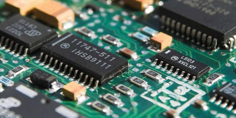
When a PCB is said to be subjected to hardware design, it simply means that it has to do with the process of picking the physical properties of the Printed Circuit Board (PCB). These properties range from the components, making of the schematics, and the designs of the microchips and the circuit board.
The PCB hardware design process also encompasses the selection or brainstorming on the right types of components or parts to use for the circuit board design. Most often, your experience is required here and if you need help, you can always count on a circuit board engineer – Hillman Curtis.
We will help you get the most out of the PCB design process by offering the following services:
- Coming up with ideas and drafting different designs for the Printed Circuit Board (PCB).
- Making of a few prototypes to test the accuracy of the designed PCBs.
- We will also get involved in the manufacturing of the circuit board’s hardware.
- You can count on us to test the boards before shipping and supervise the entire component placement process.
How Relevant is PCB Hardware Design?
It will interest you to know that you can make the most out of your PCBs, if you toe the path of using the hardware design process.
It is also important to point out that the overall concept of PCB design falls under the Hardware (HW) aspect of engineering. By this, it has a lot of facets, including but not limited to:
- Manufacturing
- Electrical
- Testing
- Mechanical
- Systems and;
- Software
What is the PCB Hardware Design Process?
For a PCB to be designed using the hardware process, a lot of hands need to be on deck – the circuit board. The following persons have a role to play:
- Electrical Designer
- Electrical Engineer
- Mechanical Engineer
These three sets of persons come in with their services or skillsets at different points in the circuit board design.
Here is a detailed breakdown of the steps to be taken when making a PCB hardware design:
1. Moving from Schematic to PCB
The first step is to translate the idea of the ideal circuit board from paper to reality. For this to happen, the services of the electrical engineer are needed. Also called the electronics engineer, the engineer helps to create the schematics of the circuit board.
Once this has been done, the PCB will be passed on to the mechanical engineer, who provides the envelope or physical packaging for the board. This packaging also comes with the physical constraints and requirements for the board.
Once the process above is completed, the mechanical data/information derived therein will be fed into the PCB’s layout.
This brings us to the doorstep of the third man in the mix – the electrical designer. Also known as the layout specialist, the electrical designer helps to make the layout for the Printed Circuit Board (PCB).
2. How the Electrical Inputs and Physical Constraints Relate in PCB Hardware Design

We would like to point out some important points about how the different elements come together to bolster the hardware design of circuit boards.
The first point is that the hardware is created or derived from the mechanical definitions and constraints, which are fed into the circuit board’s layout.
The second point is that the data being fed into the PCB layout contain both the electrical input/requirements and the combination of the electrical and the physical constraints. The idea is for the electrical inputs to include the schematics, such as diagrams and graphical symbols that depict the electronic circuit. On the other hand, the electrical and physical constraints are meant to meet the end-product or finished PCB’s requirements/definitions/design rules.
The Structure of PCB Hardware Design
Before you can say that you have followed the hardware design process of making PCBs, you must have factored in different processes.
Due to the fact that several inputs and requirements are sourced from multiple facets, the PCB’s hardware design must meet the following requirements:
1. Architecture Definition
This has to do with the system-level requirement that enables the definition or structuring of the primary basis for the board.
2. Mechanical and Electrical Requirements
These include the mechanical, electrical, software and system requirements for the board. It also includes the test constraints and requirements for making the PCB’s hardware design.
3. Circuit Board’s Integrity and Compliances
This involves the testing of the board against the prevailing design rules. It also covers the following:
- Power Integrity: also called PI, it x-rays the circuit board’s ability to measure up with the basic power requirements.
- Signal Integrity: a Printed Circuit Board (PCB) cannot thrive if it doesn’t provide the relevant signals. This is the reason for the Signal Integrity (SI) requirements to validate the capability to measure up with the required signal transmission rate and processes.
- Electromagnetic Compatibility: the EMC has to do with the board’s possible exposure to electromagnetic waves and the capabilities of preventing the same from causing issues for its performance.
- Design for Manufacturability (DFM): this has to do with the board’s compliance with both the design rules and the Design for Manufacturability (DFM) requirements. These are laid-down guidelines or processes expected of the circuit board to perform optimally after the hardware design.
- Component Sourcing: this leans more towards the supply chain process. It has to do with the processes of sourcing the components for the board.
1. What Next After PCB Hardware Design?
Following the steps in the hardware design process, you should have laid the ground for the next steps for the PCB’s design.
After that has been completed, the next step is the designing of the schematics. The following processes are used to actualize it:
The Use of an EDA Tool
The EDA is the short form of Electronics Design Automation. It refers to the use of software to facilitate the real-time designing of a Printed Circuit Board (PCB) or consumer electronics.
Thus, you need a good EDA tool to create the schematics for the circuit board. Some of the popular options you can find out there are:
Choosing the EDA tool/software sets the ground for the next stages. These are the steps to maximizing the schematic creation process:
Circuit Creation
There is a different between the circuit and the circuit board. The thin line of difference is that the circuit is a graphical representation of the board, while the circuit board is an embodiment of the different graphical representations, as well as the components mounted on these representations to perform one function or the other in the board.
Therefore, after the creation of the schematic symbol, the next step that follows is to create the circuit.
Reviews
Before moving to the next stage, go through the entire schematic creation process to be sure nothing important was left out.
2. Start Designing Your PCB
You are now good to go with designing the PCB. This is where you need to pay careful attention, but if the process is skipped or not followed to the latter, you can be sure of getting a less-functional board.
The following are important elements of the Printed Circuit Board (PCB) design process:
Footprint Creation
The footprint here refers to the pathway or the strategic places where the components are mounted on the circuit board.
The creation should cover the different points where the components are to be placed on the board. Provisions should also be made for the pathways for routing the signals.
Part Placement
With the footprint created, you can now start placing or mounting the components or parts where they are designated to be on the board.
Make the Circuit Layout
This is an overview of how the board would turn out to be at the end of the day. Note that depending on the complexity of the design, you might have to carry out series of Electromagnetic Interference (EMI) and Signal Integrity (SI) analyses.
Testing
The PCB would now be tested to confirm if all the components are working as they should.
Finishing and Shipping
Hillman Curtis will put final touches on the board and start making preparations to ship it to you, anywhere you are in the world.
How to Approach PCB Hardware Design
To get the most out of the design, you must approach the configuration of a hardware PCB the right way. These tips will guide you through the PCB design process:
1. Set the Right Expectations
Many hardware PCB design enthusiasts are hopeful to get it right the first they tried. While there may be nothing bad about being optimistic, there is also the place of having a right mindset.
The fact is that the design is subject to flops and might not turn out to be done rightly the first few times. With this in mind, you wouldn’t be overly concerned if the design doesn’t come out as expected.
2. Be Upfront about the Expectations
This works best if you are contracting a professional PCB hardware designer, in the name of Hillman Curtis. We appreciate it when you are upfront or clear about your expectations. It helps us to figure out better ways to meet up with your requirements.
3. Multiple Collaborations
As you could deduce from where we talked about the different persons involved in the design, you could see that different collaborations are needed.
As a multi-discipline and multi-domain collaboration circuit board design process, it requires for the appropriate integrations to be made.
PCB hardware design also requires the constant, bidirectional interfacing between all the persons involved in the design – electrical designer, electrical engineer and mechanical engineer.
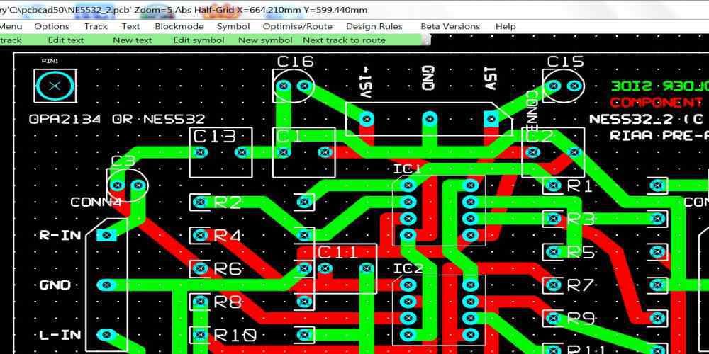
PCB Layout Design vs. Schematic Design
Have in mind that both the design of the schematics and the layout are two common processes used in the build-up to PCB hardware design.
However, they are not one and the same. Here are some of the clear differences between the two:
1. Design Conversion
With the help of the schematics, we can make a transition from the schematic to PCB. This conversion can also be implemented across different facets/EDA tools.
2. Testing Processes
For the hardware design, a lot of testing procedures are used. These range from Design for Serviceability (DFS), Design for Manufacturability (DFM), and Design for Testability (DFT).
However, when it comes to PCB layout, the consideration is mostly on the making of how the board appears at the end of the day, than testing the processes.
3. Parts Sourcing and Stack-Up
The next difference between PCB schematics and layout is that the former often overs the creation of the parts’ symbols and the provision of a library or database where such symbols can be accessed. At Hillman Curtis, we use your Bill of Materials (BOMs) to source accurate pars for your board’s design.
On the other hand, the PCB layout process typically covers the creation of ultra-high density and high layer count PCBs.
Conclusion
The PCB hardware design process is not as technical as it appears to be. It is a three-step process, starting with the selection of the different components and the development of functionalities for each of the blocks, followed by the capturing/making of the schematics and finally‚ the designing of your Printed Circuit Board (PCB).
