The PCB layout of Arduino Uno is a crucial aspect of its design that determines the performance and functionality of the board. PCB layout refers to the arrangement of components, traces, and other elements on the board, which affects the electrical and mechanical properties of the circuit. A well-designed PCB layout can ensure optimal signal integrity, minimize noise and crosstalk, and improve the overall reliability and manufacturability of the board.
The Arduino Uno is a popular microcontroller board that is widely used for various DIY projects, prototyping, and educational purposes. Its compact size, low cost, and ease of use make it an ideal platform for beginners and experienced users alike. However, designing a PCB layout for Arduino Uno requires careful consideration of several factors such as the placement of components, the routing of traces, and the selection of materials. A good PCB layout can help to avoid common issues such as electromagnetic interference (EMI), thermal problems, and mechanical stress that can affect the performance and longevity of the board.
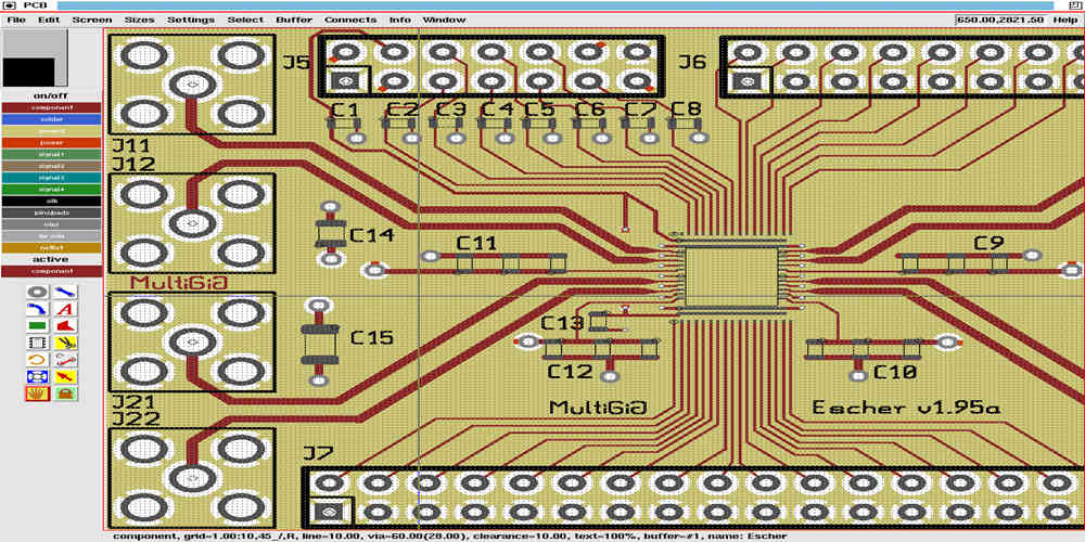
Overview of PCB Layout
When designing a printed circuit board (PCB) layout for the Arduino Uno, it is important to consider the placement of components and routing of traces. The PCB layout affects the performance, reliability, and manufacturability of the board.
Components Placement
The placement of components on the PCB should be optimized for functionality, ease of assembly, and space utilization. The Arduino Uno has a variety of components, including microcontroller, voltage regulator, USB interface, and more. These components should be placed in a logical and organized manner, taking into account their electrical connections and physical dimensions.
To aid in component placement, it is recommended to use a grid system and to group related components together. Additionally, critical components should be placed away from noise sources and heat sources, and proper clearance should be provided between high voltage and low voltage components.
Routing
The routing of traces on the PCB should be optimized for signal integrity, power distribution, and manufacturability. The Arduino Uno has a variety of signals, including digital, analog, and power. These signals should be routed in a way that minimizes noise, crosstalk, and voltage drop.
To aid in routing, it is recommended to use a layer stackup that separates signals and power planes. Additionally, critical signals should be routed first, followed by less critical signals. Proper clearance should be provided between traces and components, and vias should be used to connect different layers.
In conclusion, the PCB layout of the Arduino Uno should be carefully designed to ensure optimal performance, reliability, and manufacturability. By considering the placement of components and routing of traces, a high-quality PCB can be produced.
Design Considerations
When designing a printed circuit board (PCB) layout for an Arduino Uno, there are several important considerations to keep in mind. These include power supply, grounding, and signal integrity.
Power Supply
The power supply is a critical component of any PCB design. The Arduino Uno requires a 5V power supply, which can be provided by a USB cable or an external power source. When designing the PCB layout, it is important to ensure that the power supply is stable and free from noise. This can be achieved by adding decoupling capacitors near the power supply pins on the Arduino Uno.
Grounding
Grounding is also an important consideration when designing a PCB layout for an Arduino Uno. The ground plane should be designed to provide a low-impedance path for current flow. This can be achieved by using a solid ground plane and connecting all ground pins on the Arduino Uno to this plane. Additionally, it is important to ensure that the ground plane is free from noise, which can be achieved by using a ground pour around the signal traces.
Signal Integrity
Signal integrity is critical for reliable operation of the Arduino Uno. To ensure good signal integrity, it is important to keep the signal traces as short as possible and minimize the number of vias. Additionally, it is important to ensure that the signal traces are routed away from noisy components, such as the power supply and high-frequency components.
In summary, designing a PCB layout for an Arduino Uno requires careful consideration of the power supply, grounding, and signal integrity. By following these guidelines, designers can ensure that their PCB layout provides reliable and stable operation for the Arduino Uno.
Arduino Uno Schematic

The Arduino Uno is a popular open-source microcontroller board that is widely used for various projects. Its schematic is an essential reference for anyone who wants to understand how the board works and how to design their own custom boards based on the Uno.
The schematic of the Arduino Uno is relatively simple and straightforward. It consists of a few main components, including the ATmega328P microcontroller, the USB-to-serial converter, and the power supply circuitry.
The ATmega328P microcontroller is the heart of the Arduino Uno. It is responsible for executing the user’s code and controlling the board’s various peripherals, such as the digital and analog inputs and outputs, PWM outputs, and more.
The USB-to-serial converter is used to communicate with the computer and upload code to the board. It converts the USB signals from the computer into serial signals that the ATmega328P can understand.
The power supply circuitry includes a voltage regulator that converts the input voltage to a stable 5V, which is used to power the board and its components. There is also a 3.3V voltage regulator that provides power to some of the board’s peripherals.
Overall, the Arduino Uno schematic is a useful reference for anyone who wants to understand how the board works and how to design their own custom boards based on the Uno. With its simple and straightforward design, it is easy to follow and understand.
PCB Layout Steps
Creating a New Project
Before starting the PCB layout, create a new project in your PCB design software. In the project, set the board size and create a schematic of the Arduino UNO. Make sure to include all the components and connections.
Placing Components
Once the schematic is complete, place the components on the PCB board. Keep in mind the placement of the components should be such that it minimizes the length of the traces. It is also important to keep the components spaced out to avoid any short circuits.
Use a grid to ensure that the components are placed accurately. It is recommended to place the components in a logical order, such as starting from the power supply, then the microcontroller, and then the other components.
Routing
After placing the components, it is time to route the connections. Start by routing the power supply and ground traces. Then, route the traces for the microcontroller and other components.
Make sure to keep the traces as short as possible and avoid crossing them. Use vias to switch between the top and bottom layers of the PCB board. It is also important to ensure that the traces have sufficient clearance from each other to prevent any short circuits.
In conclusion, by following these steps, you can create a well-designed PCB layout for your Arduino UNO.
