Table of Contents
TogglePrinted circuit board (PCB) trace design is a crucial aspect of electronic circuit design. It involves designing and laying out the copper traces that connect various components on a PCB. The quality of the trace design can have a significant impact on the performance, reliability, and cost of the final product.
The design of PCB traces requires careful consideration of various factors such as the electrical properties of the materials used, the intended signal frequencies, and the physical layout of the circuit. The goal is to minimize signal distortion, crosstalk, and noise while ensuring that the traces can handle the required current and voltage levels. Proper trace design can also help reduce electromagnetic interference (EMI) and improve signal integrity.

Basics of PCB Trace Design
Trace Width and Spacing
The width and spacing of a PCB trace are critical factors in the design of a printed circuit board. The trace width determines the amount of current that can flow through the trace without overheating, while the spacing between traces affects the overall impedance of the circuit.
When designing a trace, it’s important to consider the amount of current that will flow through it. The trace width should be wide enough to handle the current without overheating, but not so wide that it takes up too much space on the board. A good rule of thumb is to use a trace width that is at least 3 times the thickness of the copper layer on the board.
The spacing between traces is also important, as it affects the overall impedance of the circuit. If the spacing between traces is too small, the impedance of the circuit will be too low, which can lead to signal distortion and interference. On the other hand, if the spacing is too large, the impedance will be too high, which can lead to signal loss.
Trace Length and Impedance
The length of a PCB trace also affects the overall impedance of the circuit. As the length of the trace increases, the impedance of the circuit also increases. This can lead to signal distortion and interference, especially at high frequencies.
To minimize the effects of trace length on impedance, it’s important to keep traces as short as possible. If longer traces are necessary, they should be designed with a controlled impedance to minimize signal distortion. This can be achieved by using a trace with a specific width and spacing, or by using a transmission line with a specific impedance.
In conclusion, designing PCB traces requires careful consideration of trace width, spacing, length, and impedance. By following these basic principles, designers can create circuits that are reliable, efficient, and free from signal distortion and interference.
Signal Integrity Considerations

Signal Reflections and Crosstalk
When designing a PCB trace, it’s essential to consider signal reflections and crosstalk. Signal reflections occur when a signal encounters an impedance change, causing a portion of the signal to reflect back towards the source. This can lead to signal distortion, noise, and even damage to the components.
Crosstalk, on the other hand, happens when the electromagnetic field of one trace interferes with the signal of another trace. This can lead to signal coupling and noise, which can affect the overall performance of the circuit.
To minimize signal reflections and crosstalk, here are some best practices to follow:
- Keep traces as short as possible
- Use proper termination techniques
- Ensure that there is adequate spacing between traces
- Use a ground plane to reduce electromagnetic interference
Termination Techniques
Termination techniques are crucial for reducing signal reflections and ensuring that signals are properly transmitted. There are several termination techniques to choose from, including:
- Series Termination: A resistor is placed at the end of the trace to match the characteristic impedance of the trace and reduce signal reflections.
- Parallel Termination: A resistor is placed in parallel with the receiver to provide a low impedance path for the signal and reduce reflections.
- AC Termination: A capacitor is placed in series with the resistor to provide a low impedance path for high-frequency signals.
Choosing the right termination technique depends on the specific requirements of the circuit. It’s important to consider factors such as the signal frequency, the trace length, and the characteristic impedance of the trace.
In conclusion, signal integrity is a critical consideration when designing PCB traces. By following best practices and using proper termination techniques, you can minimize signal reflections and crosstalk, ensuring that your circuit performs as intended.
Power Integrity Considerations
Power Plane Design
When designing a PCB trace for power integrity, it is important to consider the power plane design. The power plane should be designed to provide low impedance paths for the power supply current. This can be achieved by using multiple power planes, with each plane providing a dedicated power supply to a specific section of the circuit.
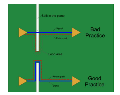
A common approach is to use a split power plane design where one plane is dedicated to the power supply and the other plane is used for the ground. This approach helps to reduce the loop area and minimize the inductance of the power supply and ground connections.
Decoupling Capacitors
Decoupling capacitors are another important consideration for power integrity. These capacitors are placed close to the power pins of the ICs to provide a low impedance path to ground for high-frequency noise. The value of the decoupling capacitor should be selected based on the frequency range of the noise and the current requirements of the IC.
It is important to place the decoupling capacitors as close as possible to the power pins of the ICs. This helps to reduce the loop area and minimize the inductance of the power supply and ground connections.
When selecting the decoupling capacitors, it is important to consider the equivalent series resistance (ESR) and equivalent series inductance (ESL) of the capacitor. These parameters can affect the performance of the capacitor at high frequencies and should be minimized.
In conclusion, designing a PCB trace for power integrity requires careful consideration of the power plane design and the use of decoupling capacitors. By following these guidelines, you can ensure that your PCB design provides a stable and reliable power supply to your circuit.
High-Speed Design Techniques

When designing high-speed printed circuit boards (PCBs), it is essential to consider the trace and routing layout carefully. In this section, we will discuss some essential techniques for high-speed PCB trace design.
Via Placement and Routing
Via placement and routing is crucial in high-speed PCB trace design. Vias can add inductance and capacitance to the circuit, which can affect signal integrity. To minimize these effects, it is essential to place vias carefully and route traces to minimize the number of vias used.
One technique is to use blind and buried vias. These vias connect inner layers of the PCB without going through the entire board, reducing the length of the via and its impact on the signal.
Clock Routing
Clock signals are critical in high-speed PCB designs. The clock signal must be routed carefully to ensure that the signal arrives at all components simultaneously. This is known as clock skew management.
To manage clock skew, it is essential to use matched trace lengths. This technique ensures that all traces are the same length, which means that the clock signal arrives at all components at the same time.
Skew Management
Skew is the difference in arrival time of a signal at different points on the PCB. Skew can cause timing errors and affect the overall performance of the circuit. To manage skew, it is essential to use techniques such as matched trace lengths and delay lines.
Delay lines are used to introduce a delay in the signal, which helps to synchronize the signal at different points on the PCB. This technique is useful in systems where the clock signal is distributed to multiple components.
In conclusion, designing high-speed PCBs requires careful consideration of trace and routing layout. Via placement and routing, clock routing, and skew management are essential techniques to ensure the signal integrity and overall performance of the circuit.
Advanced Design Considerations

EMI/EMC Compliance
When designing PCB traces, it is important to consider electromagnetic interference (EMI) and electromagnetic compatibility (EMC) compliance. EMI can cause unwanted noise and interference in other electronic devices, while EMC ensures that the PCB does not interfere with other devices. Here are some considerations for achieving EMI/EMC compliance:
- Use a ground plane to reduce EMI and EMC.
- Keep signal traces short and straight to reduce noise.
- Use shielding to protect sensitive components from EMI.
- Use filters to reduce EMI and EMC.
Thermal Management
Thermal management is another important consideration when designing PCB traces. Overheating can cause damage to components and degrade performance. Here are some tips for managing thermal issues:
- Use a heat sink to dissipate heat.
- Place components in areas with good airflow.
- Use thermal vias to transfer heat to other layers.
- Use thermal reliefs to reduce thermal stress on components.
By considering EMI/EMC compliance and thermal management in your PCB trace design, you can ensure that your PCB performs optimally and meets industry standards.

