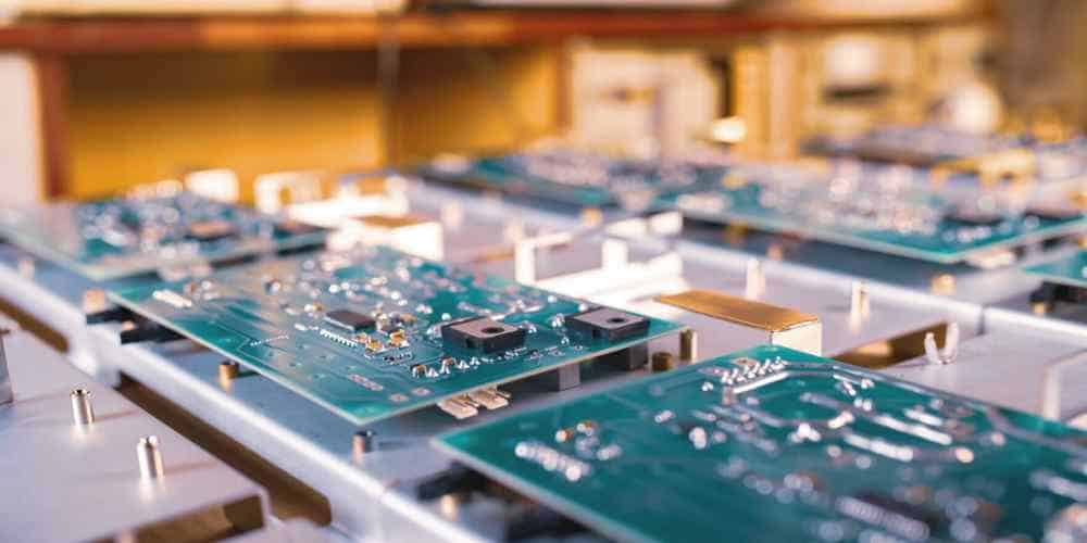
Printed circuit boards are the heart of every electronic device. Presensitized PCBs have revolutionized the electronics industry. That’s why it is cost-effective to produce high-quality PCBs. Many of you may be well aware of presensitized boards. These boards are a bit different from traditional PCB. Following content will help you to know what presensitized PCBs are, how they work, and why they are becoming increasingly popular.
What Are Presensitized PCBs?
Nowadays, if you open any electronic device, you may notice a green color board. This board is a presensitized printed circuit board. This PCB has a layer of green material however it is hard. This sensitive material is Photoresist. The Photoresist is a polymer that changes its chemical properties due to light exposure. Then the PCB is exposed to an Ultraviolet light source. As a result, it hardens the areas that have Photoresist material. As a result, the unexposed areas remain soft. Developing solutions has ability to wash unnecessary areas. As a result, you have your desired circuit board.
Key Features of Presensitized PCBs
Presensitized PCBs have many features that make them attractive for electronic device manufacturers. Some of these features are:
· High Resolution
The use of photosensitive materials on presensitized PCBs gives them a high resolution. This resolution can be as high as 25 micrometers; usually traditional PCbBs don’t have such high resolution. This is the edge of presensitized PCBs
· Accuracy
Presensitized printed circuit boards (PCBs) are highly precise. That’s why it indicates that the circuit design imprinted on the PCB aligns perfectly with the original design. This level of accuracy is accomplished through a photographic method that precludes any chance of error.
· Fast Prototyping
Prototyping has a significant place in the PCB world. The utilization of presensitized printed circuit boards (PCBs) has granted the opportunity to expedite the prototyping process, thereby resulting in a substantial reduction of the required timeframe for creating a prototype. This can be attributed to the rapid exposure of the presensitized PCBs to ultraviolet light, which instigates the formation of the desired circuit pattern with efficiency.
Manufacturing Process
Many people think the manufacturing process of these PCBs is complex, but it is not complex at all. The following steps will explain its manufacturing process in detail. The Presensitized PCB process involves following main steps however these steps are not complex.
1. Cleaning and application of the Photoresist
The first step in the manufacturing process is to clean the copper-clad board. Cleaning is crucial to remove all impurities; impurities and dust can affect the application of photoresists. In case of dust and impurities, Photoresist doesn’t stick properly, that’s why cleaning is a must. After cleaning, a Photoresist is applied to the board with the help of a spray or roller. Different manufacturers use different techniques.
2. Pre-Baking
Once the Photoresist has been applied, the board is pre-baked to ensure that the Photoresist adheres properly to the surface of the board. If Photoresist doesn’t stick to the board properly, then it will affect the PCB design.
3. Imaging
In the imaging stage, the PCB is exposed to UV light through a mask. This mask has the desired circuit pattern. As a result, UV light causes a chemical reaction in the Photoresist layer according to the cut. So the exposed part has strong adhesive Photoresist, and it’s getting hard. However, this process is a bit technical.
4. Developing
The next stage is the developing stage. The developer solution is the need of the developing stage. This step is crucial for the removal of unnecessary parts of the photosensitive layer. Developer solutions do work properly. In this way, you only have the remaining photosensitive layer on the board. This is all due to the cut of the layer. As a result, you have the desired design.
5. Etching
Etching is the final stage. It is a bit technical, that’s why it needs special attention. During the stage of etching, the printed circuit board (PCB) is fully immersed in a solution. This solution erodes the copper in the areas that are exposed. As a result, retaining the non-copper sections that shape the required circuit configuration remains available. The etching solution operates by dissolving the copper, leaving behind the impressions and pads that constitute the electrical linkages within the PCB.
Benefits Of Using Presensitized PCBs

Presensitized PCBs are part of a wide range of electronic devices, from smartphones to industrial equipment. That’s why Presensitized PCBs offer several advantages over traditional PCBs, including:
· Increased precision
Precision is the beauty of printed circuit boards. That’s why you can go for Presensitized PCBs. Presensitized PCBs provide you with very fine and precise circuit patterns. They have a higher level of accuracy than traditional PCBs. That’s why these boards are part of many devices and appliances.
· Cost-effectiveness
The presensitized PCB production process is more cost-effective than traditional PCB production methods. That’s why they are an ideal choice for the mass production of electronic devices. The manufacturing process is simple and eliminates the need for specialized equipment. That’s why it reduces the use of hazardous chemicals and complicated machinery. As a result, you get a budget-friendly PCB.
· Time-saving
The presensitized PCB production process is simple and faster. In addition, their manufacturing method is modern as compared to the traditional PCB production methods. That’s why manufacturers produce more PCBs in less time. However, production time can vary.
· Environmentally friendly
The manufacturing process is simple and doesn’t require any harsh chemicals. That’s why during the production of Presensitized PCBs, there is no harmful waste. This waste is not as harmful as traditional waste. That’s why these Photoresist PCBs are more eco-friendly.
How Presensitized PCBs Are Different from Traditional PCB
The following reasons are enough to tell you how Photoresist PCBs are different from regular PCBs.
· Great in demand
Presensitized PCBs are in great demand due to their ease of use and easy availability. In simple words, these are ready-made PCBs, and that’s why people like to use these PCBs. As a result, they are the heart of the industry.
· Different Manufacturing process
Manufacturing Processes both have quite different manufacturing processes. The main difference is Photoresist coating on Presensitized PCBs. This process requires specialized equipment and skilled technicians. In contrast, the Photoresist PCBs manufacturing process is simple. It needs only the application of Photoresist material.
· Different Levels of Customization
Both PCBs offer different levels of customization. You have less to do in terms of customization of Presensitized PCBs. Traditional PCBs have more options for customization.
· Different manufacturing Materials
A variety of materials are needed in the manufacturing of traditional PCBs. For example, fiberglass, ceramic, and epoxy. In contrast, Photoresist PCBs are typically made using a Photoresist laminate. Similarly, further processing is also different.
· Cost
Presensitized PCBs are less costly, that’s why they are in great demand. Their manufacturing process is simple and doesn’t require complex materials. On the other hand, traditional PCBs require a variety of technicalities. However, the price cannot describe quality.
· Complexity
Presensitized PCBs are generally less complex than traditional PCBs. The manufacturing process of Presensitized PCBs is simple. Materials are also simple and easily available. As a result, you get simple PCBs in one go.
· Time Required for Production
Presensitized PCBs require less manufacturing time due to the less complex process. In contrast, the traditional PCB manufacturing process is complex and requires more time.
Uses In Different Industries
· Aerospace Industry
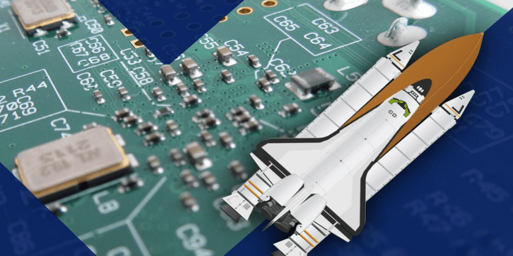
These Photoresist PCBs are the backbone of the aerospace industry to create avionics and control systems. Their precise and high-resolution capabilities make them an excellent choice for such applications.
· Medical Industry
Every day there is innovation in an incredible industry field in terms of equipment. These Presensitized PCBs are part of MRI machines, CT scanners, and ultrasound machines. The high resolution and accuracy of presensitized PCBs ensure that these machines operate professionally and correctly.
· Automotive Industry
Every automotive component or machine has a PCB, but Presensitized PCBs have a different place. The development of automotive control systems, engine management systems, and airbag control systems. These all have Presensitized PCBs the high accuracy and resolution of presensitized PCBs ensure that these systems operate efficiently and accurately.
Frequently Asked Questions
· Can presensitized PCBs be used in high-temperature applications?
Yes, Photoresist PCBs are suitable for high-temperature applications. That’s why they are part of many devices. Photoresist material makes them able to resist heat.
· Are Photoresist PCBs more expensive than traditional PCBs?
No, these PCBs are generally more cost effective than traditional PCBs. That’s why their demand is increasing day by day.
· What kind of equipment do I need to use for a presensitized PCB?
To use a presensitized PCB, you will need a UV light source, a transparency printer, or a way to create transparency in your design, a developing solution, and an etching solution. You will also need safety equipment such as gloves and goggles when working with the chemicals. In addition, you can use more modern safety equipment
Conclusion
In the coming years, you cannot expect any device without the Presensitized PCBs. That’s why these PCBs are the future of the electronics world. Undoubtedly Presensitized PCBs have revolutionized the electronics industry. They offer increased precision, cost-effectiveness, and time-saving benefits over traditional PCBs. As the demand for electronic devices continues to grow, the use of presensitized PCBs is also growing. In conclusion, you can call them the backbone of the electronic industry.
