Regulated power supply PCB layout is a crucial aspect of electronics design that ensures the stability and reliability of a power supply system. The PCB layout of a regulated power supply determines the performance of the system and its ability to meet the required specifications.
The layout of a PCB for a regulated power supply involves careful consideration of various factors such as the placement of components, the routing of traces, the use of ground planes, and the minimization of noise and interference. A well-designed layout can improve the efficiency of the power supply, reduce heat dissipation, and increase the lifespan of the components.
In this article, we will discuss the key considerations for designing a regulated power supply PCB layout, including the selection of components, the placement and routing of traces, and the use of ground planes. We will also provide practical tips and guidelines for optimizing the layout and ensuring the reliability and stability of the power supply system.

PCB Layout Basics
When designing a regulated power supply, the PCB layout is a crucial aspect that can greatly impact its performance. Here are some basics to keep in mind when creating your layout:
Component Placement
Component placement is key to creating a well-functioning power supply. It’s important to place components in a way that minimizes noise and interference. Here are some tips for component placement:
- Place high-frequency components as close to the regulator as possible to minimize noise.
- Place the input and output capacitors close to the regulator to minimize voltage spikes and drops.
- Keep heat-generating components away from sensitive components to prevent thermal interference.
Traces and Routing
The way traces and routing are laid out on the PCB can also affect the performance of the power supply. Here are some things to consider:
- Use wider traces for high-current components to reduce resistance and voltage drops.
- Keep traces as short and direct as possible to minimize noise and interference.
- Use a ground plane to provide a low-impedance ground path for the circuit.
Ground and Power Planes
A well-designed ground and power plane can help reduce noise and interference in the power supply. Here are some tips for creating a good ground and power plane:
- Use a solid ground plane to provide a low-impedance ground path.
- Place the power plane close to the ground plane to minimize electromagnetic interference.
- Use vias to connect the power and ground planes on different layers.
By keeping these basics in mind when designing the PCB layout for your regulated power supply, you can ensure that it functions as intended and provides stable, reliable power to your circuit.
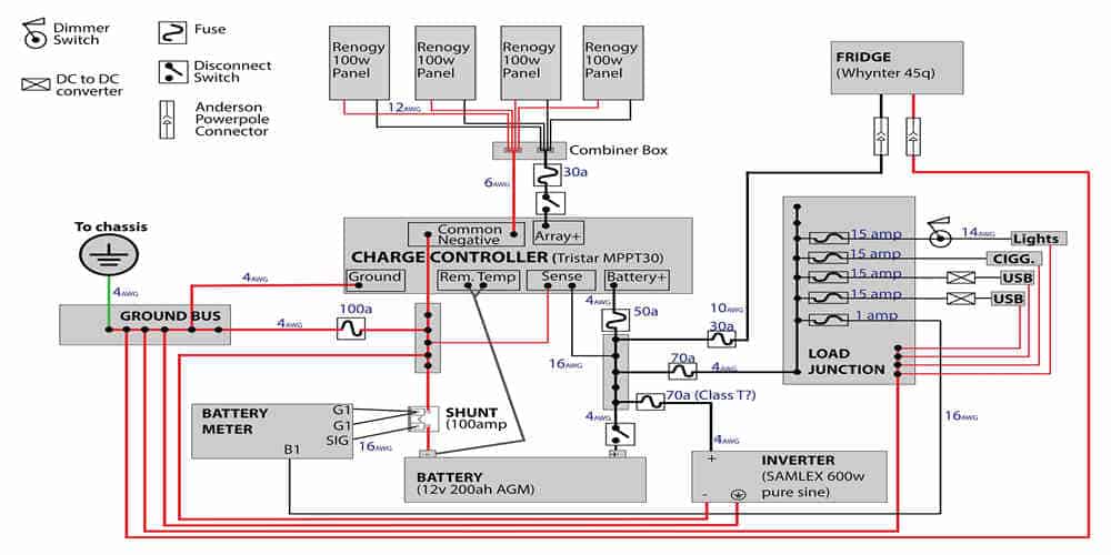
Regulated Power Supply Design

When designing a regulated power supply, it is important to consider several factors that can affect the performance and reliability of the circuit. In this section, we will discuss some key design considerations for regulated power supply PCB layout.
Voltage Regulators
Voltage regulators are an essential component of a regulated power supply, as they help regulate the output voltage and ensure a stable supply of power. When selecting a voltage regulator, it is important to consider factors such as the maximum input voltage, maximum output current, and dropout voltage.
It is also important to ensure that the voltage regulator is properly heat-sinked, as it can generate a significant amount of heat during operation. This can be achieved by using a heat sink or by mounting the regulator on a copper plane on the PCB.
Filtering Capacitors
Filtering capacitors are used to smooth out any voltage fluctuations in the power supply output, and to reduce the amount of ripple in the output voltage. When selecting filtering capacitors, it is important to consider factors such as the capacitance value, voltage rating, and ESR.
It is also important to ensure that the capacitors are properly placed and routed on the PCB, as this can affect their effectiveness. For example, it is recommended to place the capacitors as close as possible to the voltage regulator and to use short and wide traces to connect them to the regulator.
Heat Sinks
As mentioned earlier, heat sinks are an important consideration when designing a regulated power supply. They are used to dissipate heat generated by the voltage regulator and prevent it from overheating.
When selecting a heat sink, it is important to consider factors such as the thermal resistance, size, and mounting method. It is also important to ensure that the heat sink is properly connected to the voltage regulator, using thermal paste or a thermal pad.
In summary, when designing a regulated power supply, it is important to consider factors such as the selection and heat-sinking of voltage regulators, the selection and placement of filtering capacitors, and the selection and mounting of heat sinks. By taking these factors into account, you can ensure a stable and reliable power supply for your circuit.
PCB Layout Considerations for Regulated Power Supplies
Regulated power supplies are critical components in many electronic devices. The PCB layout for these power supplies is crucial to ensure stable and reliable operation. Here are some important considerations to keep in mind when designing the PCB layout for regulated power supplies.
Thermal Management
Thermal management is a critical aspect of PCB layout for regulated power supplies. Heat generated by the power supply components can cause damage to the PCB and other components. This can lead to reduced performance and even complete failure of the power supply. Therefore, it is important to design the PCB layout in such a way that it provides adequate cooling for the power supply components.
Noise Reduction
Noise can be a significant problem in regulated power supplies. Switching regulators can generate high-frequency noise that can interfere with other components on the PCB. To reduce noise, it is important to keep the power supply components as close together as possible. This reduces the length of the traces and minimizes the area of the loop formed by the power supply components.
EMI/EMC Considerations
EMI/EMC (Electromagnetic Interference/Electromagnetic Compatibility) is another important consideration when designing the PCB layout for regulated power supplies. EMI/EMC can cause interference with other electronic devices, leading to reduced performance or complete failure. To reduce EMI/EMC, it is important to ensure that the power supply components are properly shielded. This can be achieved by using a metal shield or by placing the power supply components in a metal enclosure.
In summary, when designing the PCB layout for regulated power supplies, it is important to consider thermal management, noise reduction, and EMI/EMC. By following these guidelines, you can ensure that your power supply is reliable and performs as expected.
Designing for High Current Applications
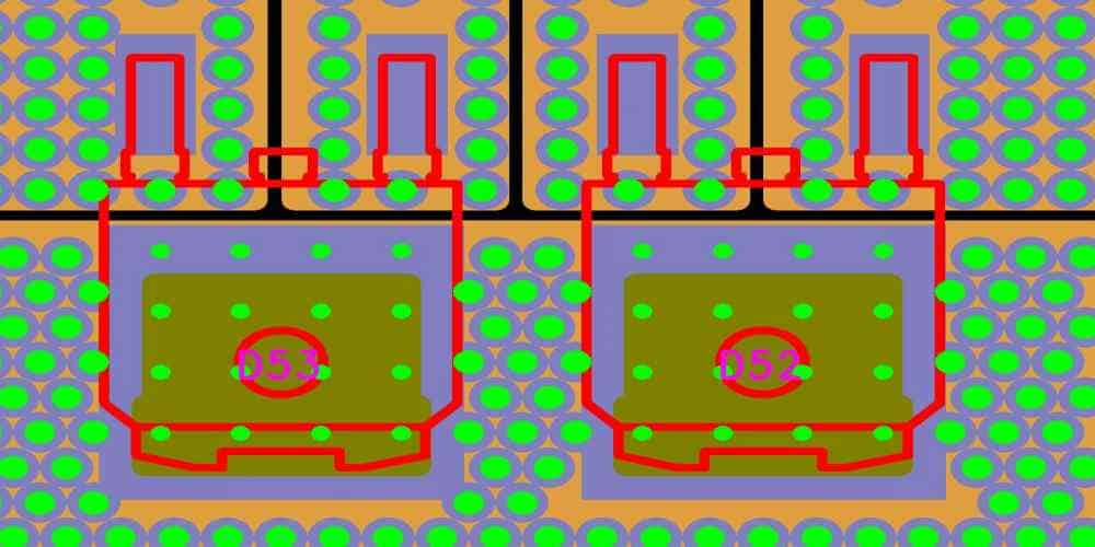
When designing a regulated power supply PCB for high current applications, there are several important considerations to keep in mind. Two key factors to focus on are trace width and thickness, as well as via placement.
Trace Width and Thickness
The trace width and thickness are crucial factors to consider when designing for high current applications. The thickness of the copper layer on the PCB plays a significant role in determining the amount of current that can be carried by the traces. The thicker the copper layer, the higher the current that can be carried.
The trace width also plays a crucial role in determining the amount of current that can be carried by the traces. The wider the trace, the higher the current that can be carried without overheating the trace. It is important to keep in mind that wider traces also take up more space on the PCB, which can impact the overall size of the design.
Via Placement
Via placement is another crucial factor to consider when designing for high current applications. Vias are used to connect different layers of the PCB together, and they can have a significant impact on the overall performance of the design.
When designing for high current applications, it is important to place vias in locations that minimize the resistance between layers. This can be achieved by placing vias as close as possible to the power and ground planes, which will provide the shortest possible path for the current to flow.
In addition, it is important to ensure that the vias are large enough to handle the current that will be flowing through them. The size of the via will depend on the amount of current that needs to be carried and the thickness of the copper layer on the PCB.
By carefully considering trace width and thickness, as well as via placement, it is possible to design a regulated power supply PCB that can handle high current applications with ease.
Testing and Troubleshooting
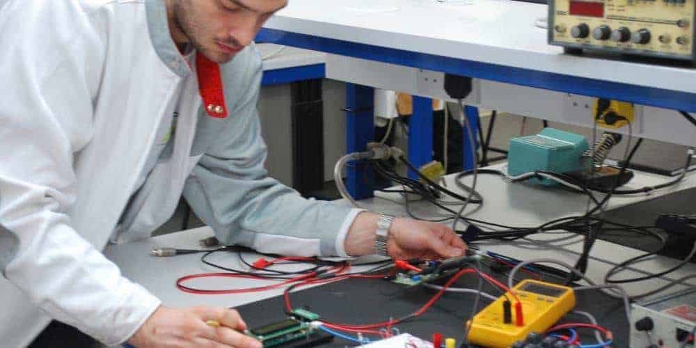
Power-On Testing
Before connecting the power supply to the load, it is essential to perform a power-on test to ensure that the circuit is working correctly. The power-on test involves checking the output voltage and current levels of the power supply. To perform the power-on test, connect the load to the power supply and turn on the power switch. Verify that the output voltage and current levels are within the specified range. If the output voltage and current levels are not within the specified range, turn off the power supply and check for any errors in the circuit.
Voltage and Current Measurements
To ensure that the power supply is providing the correct voltage and current levels, it is necessary to measure the output voltage and current. Use a digital multimeter to measure the output voltage and current. Connect the positive lead of the multimeter to the positive output terminal of the power supply, and the negative lead to the negative output terminal. Set the multimeter to measure DC voltage and current, respectively. Turn on the power supply and record the voltage and current readings.
If the voltage and current readings are not within the specified range, turn off the power supply and check for any errors in the circuit. Check the voltage regulator, capacitors, and other components for any defects or damages. Verify that the components are correctly connected and soldered. If necessary, replace the defective components and retest the power supply.
In conclusion, testing and troubleshooting are essential steps in designing a regulated power supply PCB layout. By performing power-on testing and measuring the output voltage and current, you can ensure that the power supply is working correctly. If you encounter any issues, check for errors in the circuit and replace any defective components.
