Samsung is one of the largest and most well-known electronics companies in the world, with a wide range of products that includes smartphones, televisions, and home appliances. However, Samsung is also a major player in the semiconductor industry, producing a wide range of memory chips and other components that are used in a variety of electronic devices.
One of Samsung’s key semiconductor factories is located in Hwaseong, South Korea. This facility is responsible for producing a wide range of memory chips, including DRAM and NAND flash memory. These chips are used in a variety of electronic devices, including smartphones, tablets, and computers.
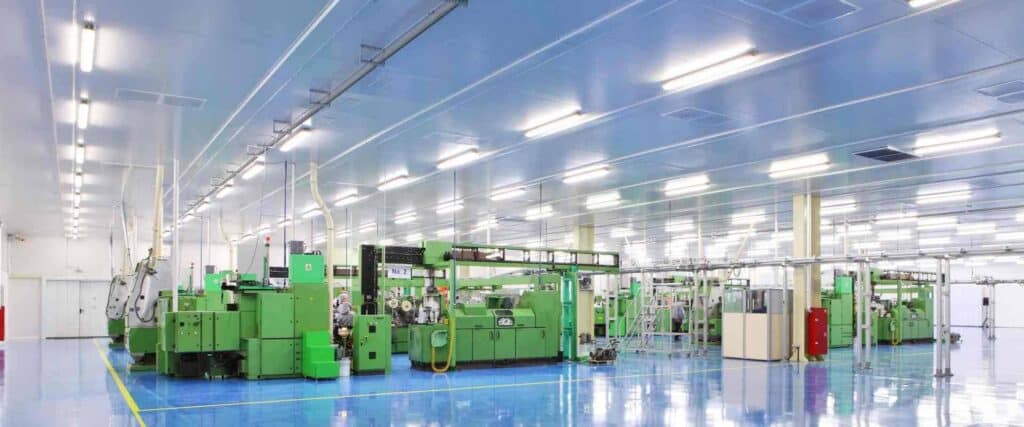
The Hwaseong factory is one of Samsung’s largest semiconductor facilities, with a total area of over 2.5 million square feet. The factory is equipped with state-of-the-art equipment and technology, allowing Samsung to produce high-quality memory chips at a large scale. The factory also employs thousands of workers, making it a key economic driver in the region.
Overview
What is Samsung Semiconductor Factory?
Samsung Semiconductor Factory is a manufacturing facility that produces semiconductor chips. Semiconductor chips are an integral part of electronic devices such as smartphones, laptops, and televisions. Samsung Semiconductor Factory is one of the largest semiconductor factories in the world and is responsible for producing a significant portion of the world’s semiconductor chips.
History of Samsung Semiconductor Factory
Samsung Semiconductor Factory was established in 1974 in South Korea. Since then, it has grown to become one of the largest semiconductor factories in the world. Samsung Semiconductor Factory has expanded its operations to other countries, including the United States, China, and Vietnam. The factory has undergone several expansions and upgrades over the years to keep up with the increasing demand for semiconductor chips.
Location of Samsung Semiconductor Factory
Samsung Semiconductor Factory has several locations around the world. The main factory is located in Giheung, South Korea. The factory covers an area of 1.6 million square meters and employs over 20,000 people. Samsung Semiconductor Factory also has facilities in Austin, Texas; Xian, China; and Ho Chi Minh City, Vietnam.
In conclusion, Samsung Semiconductor Factory is a leading manufacturer of semiconductor chips and has a significant impact on the electronics industry. With its extensive history and global presence, Samsung Semiconductor Factory is a key player in the semiconductor industry.
Production Process
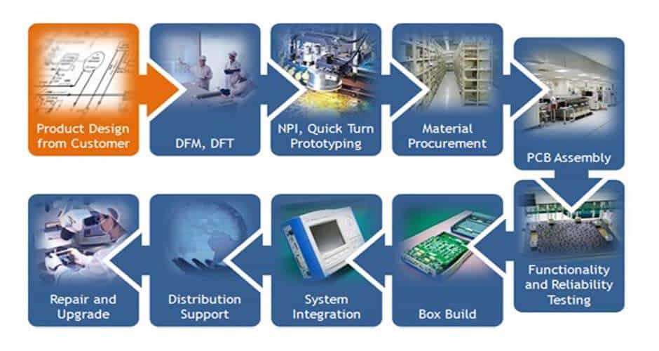
Samsung’s semiconductor factory is known for its advanced production process, which ensures high-quality products and efficient manufacturing. The production process consists of three main stages: wafer production, packaging, and testing.
Wafer Production
The first stage of the production process is wafer production. In this stage, silicon wafers are produced through a series of complex processes. The following steps are involved in wafer production:
-
Crystal Growth: A small seed crystal is placed in a crucible of molten silicon, which is then slowly cooled to form a single crystal.
-
Wafer Slicing: The single crystal is then sliced into thin wafers using a diamond saw.
-
Wafer Polishing: The wafers are polished to remove any surface defects and to ensure a smooth surface.
-
Doping: The wafers are then doped with impurities to create the desired electrical properties.
Packaging
The second stage of the production process is packaging. In this stage, the individual semiconductor devices are packaged together to form a single unit. The packaging process involves the following steps:
-
Die Attach: The semiconductor device is attached to a lead frame using a conductive adhesive.
-
Wire Bonding: Thin wires are used to connect the semiconductor device to the lead frame.
-
Molding: The semiconductor device is then encapsulated in a plastic or ceramic package.
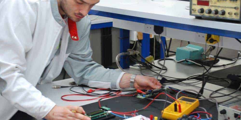
Testing
The final stage of the production process is testing. In this stage, the semiconductor devices are tested to ensure they meet the required specifications. The testing process involves the following steps:
-
Electrical Testing: The devices are tested for their electrical properties, such as voltage and current.
-
Functional Testing: The devices are tested to ensure they function correctly.
-
Quality Assurance: The devices are inspected to ensure they meet the required quality standards.
Overall, Samsung’s semiconductor factory has a highly advanced production process that ensures high-quality products and efficient manufacturing.
Technology and Innovation
Advanced Technology
Samsung Semiconductor Factory is a leader in advanced technology, constantly pushing the boundaries of what is possible. The company invests heavily in research and development to ensure that its technology is always at the forefront of the industry. One of the key areas of focus for Samsung is the development of new materials and processes that can be used to create more efficient and powerful semiconductors.
One example of Samsung’s advanced technology is its use of extreme ultraviolet (EUV) lithography. This cutting-edge technology allows for the creation of incredibly small, precise features on semiconductor wafers, enabling the production of chips with higher performance and lower power consumption.
Another area where Samsung is leading the way is in the development of 3D packaging technology. This approach involves stacking multiple layers of chips on top of each other, allowing for higher performance and more compact designs. Samsung’s 3D packaging technology is used in a wide range of applications, from mobile devices to data centers.
Investment in Research and Development
Samsung Semiconductor Factory’s commitment to innovation is reflected in its significant investment in research and development. The company has a dedicated team of scientists and engineers working to develop new technologies and improve existing ones. In 2022, Samsung spent over $18 billion on research and development, making it one of the largest R&D investors in the world.
This investment has led to a number of breakthroughs in semiconductor technology, including the development of new materials, processes, and packaging techniques. Samsung’s R&D efforts have also resulted in the creation of new products and services, such as the company’s Exynos mobile processors and its SmartSSD solid-state drives.
In addition to its own internal R&D efforts, Samsung Semiconductor Factory also collaborates with academic institutions and other companies to advance the state of the art in semiconductor technology. These partnerships help to ensure that Samsung remains at the forefront of the industry and continues to deliver innovative products and solutions to its customers.
Environmental Impact
Sustainability Efforts
Samsung Semiconductor has been implementing various sustainability efforts to reduce its environmental impact. The company has set a target to reduce greenhouse gas emissions by 70% by 2023 compared to the levels in 2008. To achieve this goal, Samsung Semiconductor has been investing in renewable energy and energy-efficient technologies. The company has installed solar panels and wind turbines at its factories to generate clean energy. In addition, Samsung Semiconductor has been using energy-efficient equipment and technologies, such as LED lighting, to reduce energy consumption.
Samsung Semiconductor has also been focusing on reducing waste and increasing recycling. The company has implemented a waste management system that separates waste into recyclable and non-recyclable materials. Samsung Semiconductor has been increasing the amount of waste that is recycled and reducing the amount of waste that is sent to landfills.
Environmental Regulations and Compliance
Samsung Semiconductor is committed to complying with environmental regulations and standards. The company has been working closely with regulatory agencies to ensure that its operations are in compliance with local, state, and federal regulations. Samsung Semiconductor has implemented an environmental management system that monitors and manages environmental risks and impacts. The company regularly conducts environmental audits to identify areas for improvement and to ensure compliance with regulations.
Samsung Semiconductor has also been working with suppliers to ensure that they comply with environmental regulations and standards. The company has implemented a supplier code of conduct that requires suppliers to comply with environmental regulations and to implement sustainability practices.
In conclusion, Samsung Semiconductor has been implementing various sustainability efforts and complying with environmental regulations to reduce its environmental impact. The company’s commitment to sustainability and environmental compliance is evident in its investments in renewable energy, energy-efficient technologies, waste management, and supplier sustainability.
Future Plans
Expansion Plans
Samsung Semiconductor is planning to expand its semiconductor factory in the near future. The company plans to invest billions of dollars to increase the production capacity of the factory. The expansion will include the construction of new buildings and the installation of state-of-the-art equipment to increase the efficiency of the production process.
The expansion plans also include the hiring of additional staff to operate the new equipment and manage the increased production capacity. The company aims to create more job opportunities for the local community and contribute to the economic growth of the region.
New Technological Developments
Samsung Semiconductor is constantly researching and developing new technologies to improve the performance and efficiency of its semiconductor products. The company is investing heavily in research and development to stay ahead of its competitors and meet the growing demand for high-quality semiconductor products.
One of the new technological developments that Samsung Semiconductor is working on is the use of artificial intelligence (AI) in the production process. The company believes that AI can help to optimize the production process and reduce the risk of errors and defects. Samsung Semiconductor is also exploring the use of 5G technology in its semiconductor products to improve connectivity and speed.
In conclusion, Samsung Semiconductor is committed to expanding its production capacity and investing in new technologies to maintain its position as a leading semiconductor manufacturer. The company’s future plans include the construction of new buildings, the installation of state-of-the-art equipment, and the development of new technologies such as AI and 5G.
