A lot of processes go into the designing and final production of Printed Circuit Boards (PCBs). One of such processes is the use of silk layer on the board.
In this article, we discuss what silk layer PCB is and how it makes all the difference in circuit board design.
What is Silk Layer in PCB?
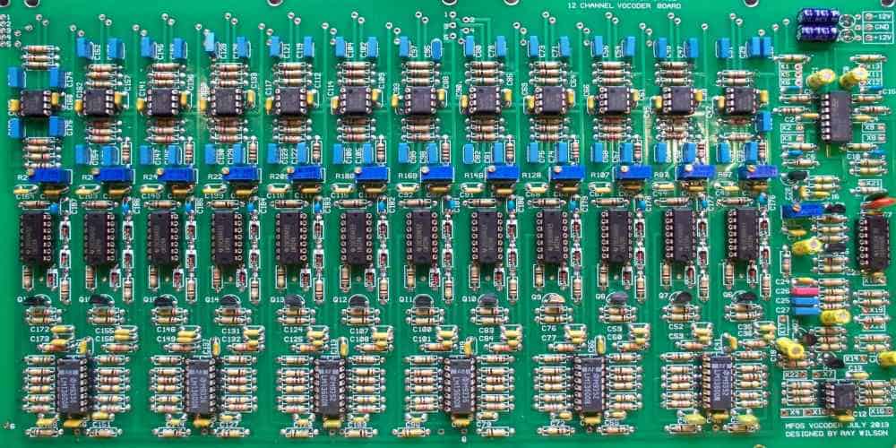
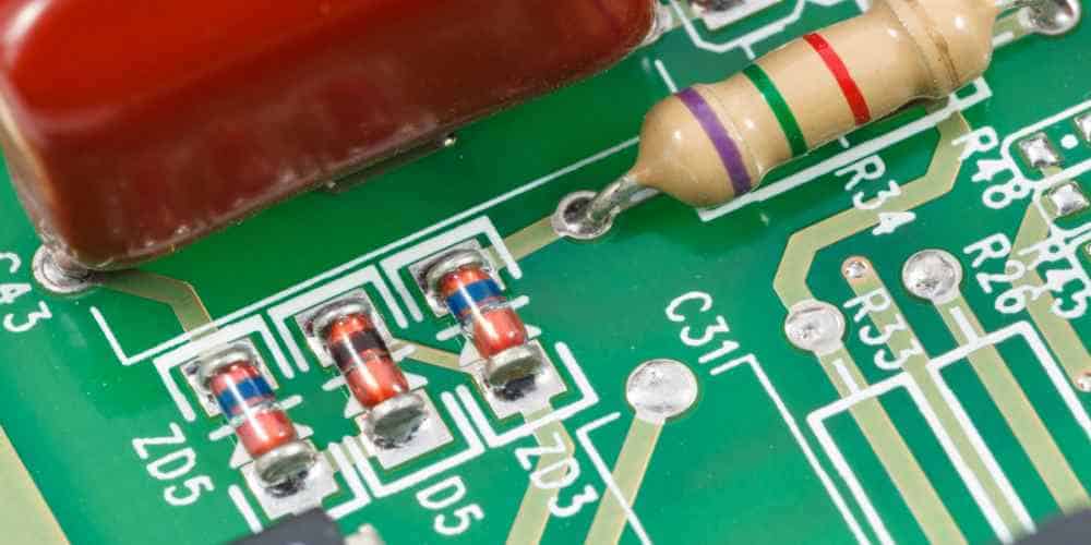
Also called silkscreen, silk layer refers to the layer of ink traces for identifying or marking out important parts of the PCB. These parts include, but are not limited to the circuit board components, symbols, logos and other essential marks.
Worthy of mentioning is that the silkscreen can also be used for other specific markings, such as pointing out the warning symbols, test points and letters.
Understanding the Position of the Silk Layer in a PCB
The position or where the layer ink traces are made is very crucial to the identification of the components, letters, numbers and other key signs and symbols on the circuit board.
By standards, the silk layer ink traces are made on the component side, which is where these identifiers are actually needed. This way, the PCB manufacturer easily identifies which components are to be mounted or are placed in those places.
However, it has become common for silkscreen to be placed in the other part of the Printed Circuit Board (PCB), which is the soldering part. However, using the silk layer for the soldering part of the circuit board could come with some additional costs.
Information Provided through Silk Layer PCB
Generally, the core information provided with PCB silkscreen is the markings or identifiers for the components.
However, you can be able to get out other pieces of information from the same printing. Here is a list of some of the information contained in the silkscreen printing:
- Component Outline: this helps in identifying or specifying where the PCB components are to be placed or mounted on the board.
- Manufacturer’s Details: this includes the version number of the PCB, and the manufacturer’s marks.
- Test Point Identification: highlighting this with the silkscreen printing helps the PCB manufacturer to take note of where to take measurements from when it is time to troubleshoot or inspect the circuit board.
- Warning Symbols: you should be able to take note of the warning symbols. Essentially, what this does for you is to help highlight the specific (higher) parameter values, such as the Power, Voltage and Current of the circuit board.
- Reference Indicator: this is a bit similar to the component identification in the sense that it helps in locating the PCB parts via the reference indicators or the designated alphabets of those components. You can also use this to identify the orientation of the components’ polarity.
What is the Best Silkscreen Printing Ink?

Manufacturers often go for the ink that makes the component identifiers easily seen. Yet, the industry-standard always comes to play and helps in picking the right silk layer ink traces.
Specially-formulated, non-conductive epoxy ink is commonly used for printing these identifiers on the Printed Circuit Board (PCB).
When it comes to the appearance, the choice differs. Although white is the most common silkscreen printing ink, it is also possible to find other colour variants. For example, some PCB designers prefer using any of the following colours:
- Black
- Yellow
- Red
- Blue and;
- Purple
It is for that reason that most PCBs are named after the silkscreen ink colour used for marking out the components’ identifiers. That is why we have the likes of blue PCB, purple PCB, and black PCB.
Nevertheless, it is up to the PCB manufacturer to decide on the type of silkscreen ink trace colour to use for the board.
The Traditional Silk Layer PCB Process
Before the advent of new silkscreen printing processes, it is common for PCB manufacturers to stick to the traditional methods. These methods include the use of polyester screens.
Here is how it works:
Polyester Screen Stretching
The first process is to have the polyester screens stretched on aluminum surfaces. That provides the “level-playing ground” for a flattened surface ahead of the printing process.
The polyester screens would then be coated with solvent-resistant emulsions.
PCB and Polyester Screen Alignment
With the coating done, the next step is to align the polyester screens with the Printed Circuit Board (PCB).
The alignment has to be parallel, as that enables the information printed where it is meant to be printed on the circuit board.
Ink Trace Application
Once it has been ascertained that the information is aligned properly, the ink trace would be applied to make a permanent marking of the information on the PCB.
Other PCB Silkscreen Printing Methods
There are a couple of other methods involved in making silkscreen prints on the PCB’s surface. These processes include but are not limited to:
1. Manual Silkscreen Printing
As the name suggests, it is a manual process of making silk layer ink traces on the PCB’s surface. The manual silkscreen printing method is used when the following conditions are prevalent:
- The PCB’s line width exceeds 0.007 inches.
- The registration tolerance is 0.005 inches.
The process includes using a stencil comprising the traces and texts. A nylon is used to make the traces, while the ink for the traces is transferred from the stencil into the laminate or layer.
2. Liquid Photo Imaging (LPI)
This process is advanced than the manual silkscreen printing method, in the sense that it provides more accuracy and legibility than the manual process does.
The accuracy is derived from the coating of the laminate with a liquid photo-imageable epoxy. The epoxy-coated laminate is then subjected to development and curing via the exposing to UV light.
3. Direct Legend Printing (DLP)
This is another method of applying the silk layer on a PCB. It involves the use of two different inks – the acrylic and the inkjet projector ink.
While the inkjet projector and acrylic ink is applied to the PCB via the CAD software, that of the acrylic ink is best used with PCBs that don’t have silver finishes. The reason is simple – the direct application of the acrylic ink to the PCB’s surface doesn’t cure easily, which is a downside for circuit boards having silver finishes.
Once the ink has been applied to the circuit board’s surface, it is to be exposed to UV light for curing.
Final Words
Silk layer PCB, also called silkscreen printing, is an excellent way to map put where components are to be placed on a circuit board. This way, excellent mapping/wiring and appropriate of the components would be possible.
