The exploration and utilization of outer space have been humanity’s long-standing dream. However, with the invention of the space Printed Circuit Board (PCB), this dream has taken a significant step forward. Space PCBs refer to specialized circuit boards explicitly designed for use in space applications that can withstand the extreme temperatures, radiation, and harsh environment of space while still reliably delivering a circuit’s electrical signals. In this article, we’ll discuss the components and analysis methods used in Space PCBs and how they enable us to explore the unknown.
Space PCB: Definition
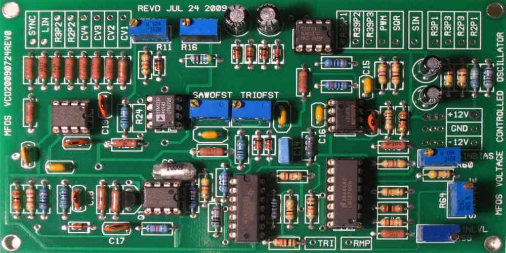
Space PCB, or Printed Circuit Board (PCB), is a specialized circuit board specifically designed for space applications. A space PCB can withstand the extreme temperatures, radiation, and harsh environment of space while reliably delivering a circuit’s electrical signals. Space PCBs usually consist of a more durable material than traditional PCBs, such as a combination of ceramic and metal, and comprise components more resistant to radiation.
Components of a Space PCB
The active components of a space PCB are responsible for the device’s operation, whereas the passive components supply the essential electrical connections.
Active Elements
A space PCB’s active components consist of microprocessors, memory, and digital logic circuits. Microprocessors are responsible for command execution and directing the overall operation of the device. Memory helps store information, including computer instructions and data. Digital logic circuits are accountable for data processing and logic operations.
ROM (Read-Only Memory), RAM (Random-Access Memory), and flash memory are components. ROM permanently stores instructions that are not available for further altering. The Space PCB stores user-modifiable data and instructions in user-modifiable RAM. Flash memory helps keep information preserved even after one switches off the power.
Digital-to-analogue (D/A) and analog-to-digital (A/D) converters help transform analog signals into digital signals and vice versa. This process enables the integration of analog signals into the digital system of the device.
Transceivers, modems, and antennas are components of communication. Transceivers are for data transmission and reception between two or more devices. For example, modems convert digital signals to analog signals for information via telephone lines. Antennas transmit and receive radio signals.
Passive Components
The role of passive components is to provide electrical connections between active components. Resistors, capacitors, inductors, and diodes are examples of passive components.
Resistors restrict the passage of current in a circuit. Therefore, we can grade them according to their resistance rating, and they are available in various sizes and shapes.
Capacitors store electrical charge and filter out signals with a high frequency.
Inductors help store energy as a magnetic field and to filter out low-frequency signals.
In addition to controlling the direction of current flow in a circuit, diodes can convert AC signals to DC signals.
Individual components have an electrical connection to the printed circuit board through connectors. We can wire them to the board or link them via a socket.
In addition to switches, relays, and transistors, other components often found on space PCBs include switches, relays, and transistors. Relays automate the switching process, whereas switches help manually control the current flow in a circuit. Transistors help in signal amplification.
To ensure that space PCBs can resist the harsh elements of space, we must utilize a range of specialized materials and methods. These include laminates and special coatings that shield components from radiation and high temperatures. In addition, heat sinks can help dissipate heat generated by the components, while vibration dampers can lessen the impacts of shock loads.
Space PCB Analysis Methods
PCB analysis involves the following four techniques:
1. Signal Integrity:

Signal integrity quantifies the quality of an electrical signal in a system. It typically helps define a system’s capacity to convey data properly through a communications medium, such as a printed circuit board (PCB). When designing a PCB, signal integrity is a crucial issue. It is essential to ensure minimal noise and crosstalk between different signals and that the PCB architecture does not distort the signal.
Following standard practices for PCB layout can increase signal integrity. For example, some techniques use shorter and wider traces, ground planes, vias, and the correct trace spacing and impedance via stitching. Additionally, you must install the decoupling capacitors in the proper positions. Furthermore, reducing the number of via-in-pad configurations and eliminating right angles in trace routing is essential.
2. Power Integrity:
Power integrity refers to the measure of a system’s power supply quality. Inadequate power integrity can lead to unreliable or malfunctioning systems; hence you must consider it while building a PCB. Inefficient layout, insufficient decoupling capacitors, insufficient voltage regulation, and excessive noise or crosstalk on power rails can all contribute to power integrity issues.
Carefully considering a PCB layout will enable you to achieve good power integrity. It is essential to ensure that power and ground lines have sufficient space between them and that voltage regulators are close to the power rails they are regulating. Please route your power rails as directly as possible and insert decoupling capacitors at suitable locations. Also, incorporate power and ground planes into the design, as they reduce power noise and crosstalk.
3. Electromagnetic Interference (EMI):
It refers to the interference caused by electrical and electronic systems and components. EMI can interfere with other systems and cause faults, leading to significant issues. Considering electromagnetic interference (EMI) while designing a PCB is crucial, as it might be challenging to regulate once your system is complete.
It is essential to adhere to layout best practices to prevent EMI on a printed circuit board (PCB). This action includes providing enough shielding, employing more considerable traces, and grounding components effectively. Additionally, power and ground planes will help you decrease noise and crosstalk. Also, please keep the number of vias minimum and position the correct decoupling capacitors at the appropriate locations. Avoiding straight angles and sharp corners while routing traces is crucial, as these might produce electromagnetic interference (EMI).
Thermal Management:
When developing and making space PCBs, thermal control is incredibly crucial. Thermal management is the technique of regulating a PCB’s temperature to keep it within a reasonable range and to prevent its components from overheating. Several methods, including good layout design, premium parts and materials, and effective cooling strategies, can help manage thermal loads.
Effective thermal management requires proper layout design since it can lessen the amount of heat produced by the PCB. In addition, we can decrease the amount of heat produced using high-quality parts and materials since they can dissipate heat more effectively. Last but not least, using effective cooling methods can help control the temperature of the PCB’s components, which can help limit the heat created.
Conclusion
In conclusion, from the above details, it is clear that designing space PCBs is more complicated and complex than designing standard PCBs. Therefore, when building a space PCB, it is crucial to analyze it by considering several things, including signal integrity, power integrity, EMI, and thermal management. With the above knowledge, we can create sturdy space PCBs that can withstand the harsh conditions of space by employing the proper materials and components, adhering to layout best practices, and using efficient cooling techniques.
