Table of Contents
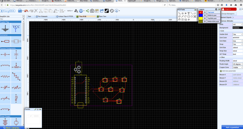
ToggleSwitching power supply PCB layout is a crucial aspect of designing a power supply. The layout of the PCB can significantly affect the performance and efficiency of the power supply. A well-designed PCB layout can reduce electromagnetic interference (EMI), improve thermal management, and increase the reliability of the power supply.
One of the primary considerations when designing a switching power supply PCB layout is the placement of components. The layout should be optimized to minimize the length of the traces between components, reduce the loop area, and minimize the parasitic capacitance and inductance. This can help reduce EMI and improve the overall performance of the power supply. Additionally, the placement of components can affect the thermal management of the power supply, and it is important to ensure that components are placed in a way that allows for efficient heat dissipation.
Another important consideration is the routing of the traces on the PCB. The traces should be routed in a way that minimizes the loop area and reduces the parasitic capacitance and inductance. The use of ground planes and power planes can also help reduce EMI and improve the overall performance of the power supply. Additionally, the use of high-quality materials and careful attention to detail during the design and manufacturing process can help ensure the reliability and longevity of the power supply.

Basics
What is a Switching Power Supply?
A switching power supply is an electronic device that converts power from one form to another. It is commonly used to convert AC power from the wall outlet to the DC power required by electronic devices. Unlike linear power supplies, which use a transformer to convert voltage, switching power supplies use a series of electronic components to convert voltage. This makes them more efficient than linear power supplies and allows them to be smaller and lighter.
PCB Layout Design
The PCB layout design is a crucial aspect of switching power supply design. The layout of the components on the PCB can have a significant impact on the performance of the power supply. The layout must be designed to minimize noise, reduce the risk of electromagnetic interference (EMI), and ensure that the power supply operates reliably.
There are several key considerations when designing the layout of a switching power supply PCB. These include:
-
Component placement: The placement of components on the PCB can have a significant impact on the performance of the power supply. Components should be placed to minimize noise and reduce the risk of EMI.
-
Trace routing: The routing of traces on the PCB can also impact the performance of the power supply. Traces should be routed to minimize noise and reduce the risk of EMI.
-
Grounding: Proper grounding is essential for the reliable operation of a switching power supply. The ground plane should be designed to minimize noise and reduce the risk of EMI.
-
Thermal management: Switching power supplies can generate a significant amount of heat. Proper thermal management is essential to ensure that the power supply operates reliably.
In summary, the PCB layout design is a crucial aspect of switching power supply design. The layout must be designed to minimize noise, reduce the risk of EMI, and ensure that the power supply operates reliably. Proper component placement, trace routing, grounding, and thermal management are all essential considerations when designing the layout of a switching power supply PCB.
Key Elements of PCB Layout Design

When designing a switching power supply PCB layout, there are several key elements that must be considered to ensure optimal performance and reliability. These include component placement, routing, grounding, and decoupling capacitors.
Component Placement
The placement of components on the PCB can have a significant impact on the performance of the switching power supply. It is important to place components in a way that minimizes noise and interference, while also ensuring efficient and effective power delivery.
Some key considerations for component placement include:
- Placing high-frequency components as close to the power supply IC as possible
- Separating noisy components from sensitive components
- Placing components in a way that minimizes the length of the traces between them
- Ensuring that components are placed in a way that allows for efficient heat dissipation
Routing
The routing of traces on the PCB is another important element of the design process. Proper routing can help to minimize noise and interference, while also ensuring that power is delivered efficiently and reliably.
Some key considerations for routing include:
- Keeping traces as short as possible
- Minimizing the number of vias used in the design
- Ensuring that traces are wide enough to handle the current being carried
- Using a ground plane to help minimize noise and interference
Grounding
Grounding is a critical element of any PCB design, and it is particularly important in switching power supply designs. Proper grounding can help to minimize noise and interference, while also ensuring that the power supply operates reliably and efficiently.
Some key considerations for grounding include:
- Using a ground plane to help minimize noise and interference
- Ensuring that all ground connections are made as short and direct as possible
- Avoiding ground loops that can cause noise and interference
Decoupling Capacitors
Decoupling capacitors are critical components in switching power supply designs, as they help to filter out noise and ensure stable power delivery. Proper placement and selection of decoupling capacitors is essential for ensuring optimal performance and reliability.
Some key considerations for decoupling capacitors include:
- Placing decoupling capacitors as close to the power supply IC as possible
- Using multiple decoupling capacitors of different values to filter out noise across a range of frequencies
- Ensuring that the decoupling capacitors are rated for the appropriate voltage and current
Overall, the key elements of PCB layout design for switching power supplies include careful component placement, efficient routing, proper grounding, and effective use of decoupling capacitors. By considering these elements during the design process, it is possible to create a power supply that delivers reliable and efficient performance.
Tips for Switching Power Supply PCB Layout Design

Keep High-Current Traces Short
High-current traces can cause voltage drops, EMI, and heat buildup. To avoid these issues, keep high-current traces as short as possible. Use wider traces to reduce resistance and increase current-carrying capacity. Place the high-current components close to each other to minimize the length of the traces. Consider using a multilayer PCB to route high-current traces on inner layers to reduce the loop area and minimize EMI.
Minimize Switching Noise
Switching power supplies generate high-frequency noise that can interfere with other circuits and cause EMI. To minimize switching noise, place the switching components, such as the MOSFET and the diode, close to each other and use short traces to connect them. Use a ground plane to provide a low-impedance return path for the switching current. Place the input and output filter capacitors close to the switching components to provide a low-impedance path for the high-frequency noise.
Avoid Ground Loops
Ground loops can cause noise, EMI, and ground potential differences that can damage the components. To avoid ground loops, use a star ground topology, where all the ground connections converge at a single point. Do not connect the input and output ground planes directly, instead, connect them through a ferrite bead or a small-value resistor to provide a high-frequency path and reduce the ground loop area. Use separate ground planes for digital and analog circuits to prevent the digital noise from interfering with the analog circuits.
By following these tips, you can design a switching power supply PCB layout that is efficient, reliable, and low-noise.
Common Mistakes in Switching Power Supply PCB Layout Design

Insufficient Clearance
One of the most common mistakes in switching power supply PCB layout design is insufficient clearance. This mistake can cause short circuits and other problems that can damage the power supply and the circuit it powers. To avoid this mistake, it is important to ensure that there is enough clearance between the components on the PCB. This can be achieved by following the manufacturer’s recommendations for component placement and spacing, and by using a PCB design tool that includes built-in clearance checks.
Improper Grounding
Another common mistake in switching power supply PCB layout design is improper grounding. This can cause noise and other problems that can affect the performance of the power supply and the circuit it powers. To avoid this mistake, it is important to ensure that the ground plane is properly connected and that all components are grounded correctly. This can be achieved by following the manufacturer’s recommendations for grounding and by using a PCB design tool that includes built-in grounding checks.
Inadequate Thermal Management
Inadequate thermal management is another common mistake in switching power supply PCB layout design. This mistake can cause components to overheat and fail, which can damage the power supply and the circuit it powers. To avoid this mistake, it is important to ensure that there is adequate thermal management on the PCB. This can be achieved by using heat sinks, thermal vias, and other techniques to dissipate heat from the components. It is also important to follow the manufacturer’s recommendations for component placement and spacing to ensure that there is enough room for proper thermal management.
In conclusion, switching power supply PCB layout design requires careful attention to detail to avoid common mistakes. By following the manufacturer’s recommendations for component placement, spacing, grounding, and thermal management, and by using a PCB design tool that includes built-in checks for these factors, designers can create high-quality, reliable power supplies that meet the needs of their applications.

