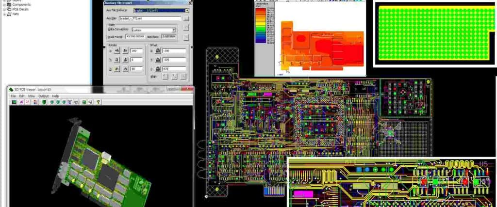
Tone control PCB layout is an essential aspect when designing audio circuits. It is the process of arranging and connecting components on a printed circuit board (PCB) to ensure the best possible sound quality. A well-designed PCB layout can help reduce noise, distortion, and interference, resulting in a cleaner and more accurate sound output.
One crucial factor to consider when designing the PCB layout is the signal path. The signal path is the path that the audio signal takes as it travels through the circuit. A well-planned signal path can help reduce the length of the audio signal path, minimizing the risk of noise and interference. Additionally, a well-planned signal path can also help reduce the number of vias and traces, which can help improve the overall sound quality.
Another factor to consider when designing the PCB layout is the placement of components. Placing components in the right position can help reduce noise and interference. For instance, placing the power supply components away from the signal path can help minimize the risk of noise. Similarly, placing the input and output connectors away from each other can help reduce interference. Overall, a well-designed PCB layout can help improve the sound quality of an audio circuit.
Tone Control PCB Layout Basics
When designing a tone control PCB layout, there are several important considerations to keep in mind. In this section, we’ll cover the basics of PCB layout design, including grounding and power distribution, signal traces, and component placement.
PCB Layout Design Considerations
The layout of a PCB can have a significant impact on the performance of the circuit. When designing a tone control PCB, it’s important to consider the following:
- Size: The size of the board should be appropriate for the circuit and the enclosure it will be housed in.
- Trace routing: The routing of traces should be optimized for signal integrity and noise reduction.
- Component placement: Components should be placed in a logical and efficient manner, with consideration given to signal flow and ease of assembly.
- Grounding: Grounding should be carefully planned to minimize noise and interference.
Grounding and Power Distribution
Grounding and power distribution are critical aspects of PCB layout design. Proper grounding can help minimize noise and interference, while effective power distribution can ensure that all components receive the necessary power.
To achieve good grounding, it is important to:
- Use a single point ground for all components.
- Keep the ground plane as large as possible.
- Separate analog and digital ground planes.
- Avoid ground loops.
When it comes to power distribution, it is important to:
- Use a power plane for even distribution of power.
- Keep the power plane as large as possible.
- Use multiple vias to connect the power plane to the ground plane.
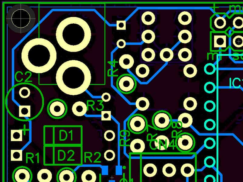
Signal Traces and Components Placement
Signal traces and component placement are also important considerations when designing a tone control PCB layout. Signal traces should be routed with care to minimize noise and interference. Components should be placed in a logical and efficient manner to ensure proper signal flow and ease of assembly.
To optimize signal traces:
- Keep signal traces as short as possible.
- Use a ground plane to reduce noise.
- Route sensitive traces away from noisy components.
To optimize component placement:
- Place components in a logical and efficient manner.
- Group related components together.
- Consider the orientation of components for ease of assembly.
By keeping these considerations in mind, you can design a tone control PCB layout that is optimized for performance, ease of assembly, and reliability.
Designing a Tone Control PCB Layout

Choosing the Right Components
When designing a tone control PCB layout, selecting the right components is crucial. The right components will ensure that the tone control circuit performs optimally. The following are some of the components that must be chosen carefully:
- Resistors: The right resistor values must be chosen to achieve the desired tone control response.
- Capacitors: Capacitor values must be chosen to achieve the desired frequency response.
- Op-Amps: The right op-amp must be chosen to ensure that the circuit operates optimally.
Schematic Design
The schematic design is the first step in designing a tone control PCB layout. The schematic diagram shows the connections between the components and how they are connected to the op-amp. The following are some of the things to consider when designing the schematic diagram:
- Component placement: Components must be placed in a logical and organized manner.
- Signal flow: The signal flow must be clear and easy to follow.
- Grounding: Proper grounding techniques must be used to minimize noise.
Layout Design
The layout design is the final step in designing a tone control PCB layout. The layout design shows the physical placement of the components on the PCB. The following are some of the things to consider when designing the layout:
- Component placement: Components must be placed in a way that minimizes noise and interference.
- Trace routing: Trace routing must be done in a way that minimizes noise and interference.
- Grounding: Proper grounding techniques must be used to minimize noise.
In summary, selecting the right components, designing a clear and organized schematic diagram, and designing a layout that minimizes noise and interference are crucial when designing a tone control PCB layout.
Testing and Troubleshooting Tone Control PCB Layout
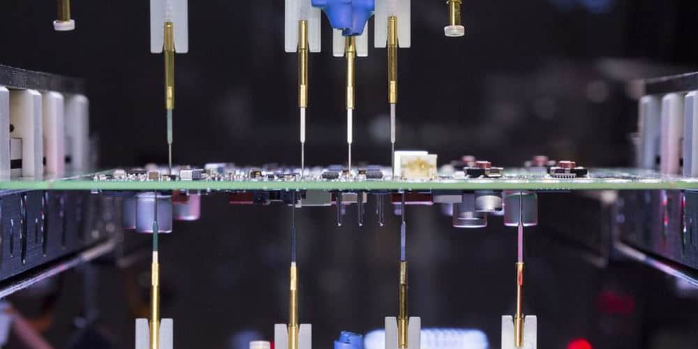
Testing the PCB Layout
Once you have finished assembling your tone control PCB, it’s important to test it to ensure that it’s working properly. This can be done using a multimeter or an oscilloscope.
To test the PCB layout using a multimeter, start by checking the voltage at the input and output terminals. If the voltage is within the expected range, move on to checking the resistance at various points on the PCB. Make sure that the resistance values match the expected values.
To test the PCB layout using an oscilloscope, connect the input signal to the input terminal of the PCB and the output signal to the output terminal. Then, use the oscilloscope to measure the input and output signals. Make sure that the output signal matches the input signal, and that the frequency response is flat across the entire audio spectrum.
Common Issues
There are a few common issues that you may encounter when testing your tone control PCB layout. These include:
- No output signal: If you’re not getting any output signal, check to make sure that the input signal is connected properly and that the power supply voltage is within the expected range.
- Distorted output signal: If the output signal is distorted, check to make sure that the resistance values are correct and that the capacitors are connected properly.
- Uneven frequency response: If the frequency response is uneven, check to make sure that the capacitors and resistors are the correct values and that they are connected properly.
Troubleshooting Tips
If you’re having trouble with your tone control PCB layout, there are a few troubleshooting tips that you can try:
- Check your connections: Make sure that all of your connections are secure and that there are no loose wires or components.
- Check your power supply: Make sure that your power supply is providing the correct voltage and that it’s stable.
- Check your components: Make sure that all of your components are the correct values and that they’re connected properly.
- Test one component at a time: If you’re having trouble pinpointing the issue, try testing each component one at a time to see if any of them are faulty.
By following these testing and troubleshooting tips, you should be able to identify and fix any issues with your tone control PCB layout.
Advanced Tips for Tone Control PCB Layout
Advanced Techniques for Noise Reduction
To reduce noise in your tone control circuit, consider the following advanced techniques:
- Grounding: Use a star grounding topology to minimize ground loop interference.
- Shielding: Shield sensitive components, such as op-amps and input jacks, from noise sources.
- Component Layout: Keep sensitive components away from high current components to minimize crosstalk and noise.
Advanced Techniques for Signal Integrity
To maintain signal integrity in your tone control circuit, consider the following advanced techniques:
- Trace Routing: Route traces as short and direct as possible to minimize signal loss and interference.
- Component Selection: Choose components with low noise and distortion characteristics for critical parts of the circuit.
- Power Supply: Use a clean and stable power supply to minimize noise and interference.
Remember to carefully consider the placement and routing of components in your tone control circuit to maximize performance and minimize noise and interference.
