The TPA3116D2 is a class-D audio amplifier that has become increasingly popular in recent years due to its high efficiency, low distortion, and low cost. However, designing a PCB layout for this amplifier can be challenging, especially for those who are new to PCB design.
One of the key considerations when designing a PCB layout for the TPA3116D2 is the placement of components. The amplifier requires a number of external components, including capacitors, resistors, and inductors, and the placement of these components can have a significant impact on the performance of the amplifier.
Another important consideration when designing a PCB layout for the TPA3116D2 is the routing of traces. The amplifier has a number of high-speed signal paths, and it is important to ensure that these traces are routed correctly to minimize noise and distortion. Proper grounding is also critical to the performance of the amplifier, and care must be taken to ensure that the ground plane is designed correctly.
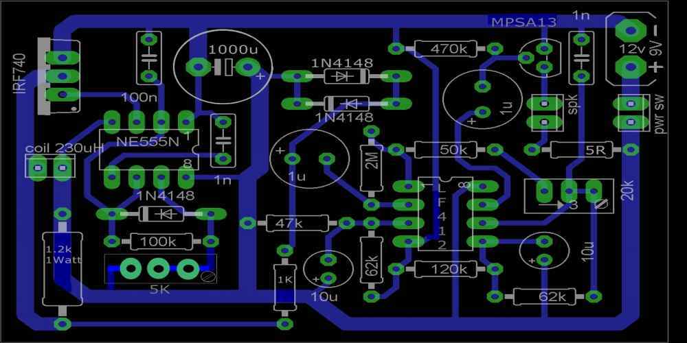
TPA3116D2 PCB Layout Basics
Choosing the Right PCB Design Software
When designing a PCB layout for the TPA3116D2 amplifier, it is important to choose the right PCB design software. The software should have the following features:
- Ability to import the TPA3116D2 datasheet and schematic
- Ability to create a multi-layer PCB layout
- Ability to place components and route traces easily
- Ability to check for design rule violations
- Ability to generate Gerber files for manufacturing
Some popular PCB design software options include Altium Designer, Eagle PCB, KiCad, and DipTrace.
PCB Design Considerations for TPA3116D2
When designing a PCB layout for the TPA3116D2 amplifier, there are several considerations to keep in mind:
- Keep the input and output traces as short as possible to minimize noise and interference
- Place the power supply components close to the amplifier to minimize voltage drop and noise
- Use a ground plane to minimize ground loops and noise
- Place the TPA3116D2 amplifier away from other high-frequency components to minimize interference
TPA3116D2 PCB Layout Guidelines
When laying out the PCB for the TPA3116D2 amplifier, it is important to follow the guidelines provided in the datasheet. Some important guidelines to keep in mind include:
- Use a four-layer PCB with a ground plane for optimal performance
- Place the power supply components close to the amplifier
- Place the input and output connectors on the same side of the PCB
- Place the TPA3116D2 amplifier away from other high-frequency components
- Keep the input and output traces as short as possible
By following these guidelines and using the right PCB design software, you can create a high-quality PCB layout for the TPA3116D2 amplifier.
TPA3116D2 PCB Layout Techniques

Single-Layer PCB Layout for TPA3116D2
When designing a single-layer PCB layout for TPA3116D2, it is important to consider the placement of the components and the routing of the traces. To minimize noise and interference, it is recommended to place the power supply components as close as possible to the TPA3116D2. Additionally, it is important to keep the traces as short as possible to reduce the risk of signal degradation.
Double-Layer PCB Layout for TPA3116D2
A double-layer PCB layout for TPA3116D2 allows for more flexibility in component placement and routing. It is recommended to place the power supply components on the bottom layer and the signal components on the top layer. To minimize interference, it is recommended to use a ground plane on the bottom layer and to keep the power and signal traces separated.
Multi-Layer PCB Layout for TPA3116D2
A multi-layer PCB layout for TPA3116D2 provides even more flexibility in component placement and routing. In addition to the recommendations for double-layer PCB layouts, it is recommended to use additional layers for power and ground planes to further reduce noise and interference. It is also recommended to use vias to connect the different layers and to keep the traces as short as possible.
When designing a PCB layout for TPA3116D2, it is important to consider the specific requirements of the application and to follow the recommended guidelines for component placement and routing. By following these guidelines, it is possible to achieve a high-quality and reliable PCB layout for TPA3116D2.
TPA3116D2 PCB Layout Best Practices
Placement of TPA3116D2 on PCB
The placement of the TPA3116D2 chip on the PCB is crucial to ensure optimal performance. It is recommended to place the TPA3116D2 as close as possible to the input and output connectors to minimize the length of the traces. Placing the chip in the center of the board can also help distribute heat evenly.
Routing Techniques for TPA3116D2 PCB Layout
When routing the traces for the TPA3116D2, it is important to keep the trace lengths as short as possible to minimize signal loss and interference. It is recommended to use a ground plane to reduce noise and provide a low impedance path for the return current.
It is also recommended to use wider traces for the power supply and ground connections to minimize resistance and voltage drops. The traces for the input and output signals should be kept separate from the power and ground traces to prevent interference.
Grounding Techniques for TPA3116D2 PCB Layout
Proper grounding is essential for the TPA3116D2 to function correctly. It is recommended to use a single point ground for the chip and connect all the ground pins to this point. This can be achieved by using a ground plane or a star ground topology.
It is also important to keep the ground traces as short as possible and avoid routing them near high-frequency signals or power traces. A ground pour can be used to provide a low impedance path for the return current and reduce noise.
In summary, by following these best practices for TPA3116D2 PCB layout, you can ensure optimal performance and reduce the risk of interference and signal loss.
