Trace PCB design is an essential aspect of modern electronics. It involves designing and implementing the electrical pathways that connect the components of a printed circuit board (PCB). These pathways, or traces, are critical to the functioning of the PCB, as they allow the flow of electrical signals between components.
The design of trace PCBs requires careful consideration of a variety of factors, including the size and shape of the board, the placement of components, and the electrical properties of the materials used. Engineers must also consider the potential for interference and noise, which can disrupt the flow of signals and cause malfunctions in the circuit. As a result, trace PCB design requires a high degree of precision and attention to detail.
Overall, trace PCB design is a crucial aspect of modern electronics, and plays a vital role in the functioning of a wide range of devices. By carefully designing and implementing the electrical pathways that connect the components of a PCB, engineers can ensure that their devices function reliably and efficiently.
Benefits of Trace PCB Design
Trace PCB design is a highly efficient and effective method of designing printed circuit boards. It offers numerous benefits, making it an ideal choice for various applications.
One of the primary benefits of trace PCB design is its ability to provide high-speed signal transmission. The design ensures that the signal travels through the shortest possible path, reducing the signal loss and maintaining the signal’s integrity. This results in improved performance and reduced noise interference.
Another benefit of trace PCB design is its ability to reduce the size of the circuit board. The design allows for the placement of components closer together, reducing the overall size of the board. This is particularly useful in applications where space is limited, such as in portable devices.
Trace PCB design also offers better thermal management. The design allows for the efficient dissipation of heat, reducing the risk of damage to the components and improving the overall reliability of the circuit board.
Additionally, trace PCB design offers better signal isolation, reducing crosstalk and ensuring that signals do not interfere with each other. This results in improved signal quality and reduced errors.
Overall, trace PCB design offers numerous benefits, making it an ideal choice for various applications. Its ability to provide high-speed signal transmission, reduce board size, improve thermal management, and better signal isolation makes it a reliable and efficient design method.
Factors to Consider in Trace PCB Design

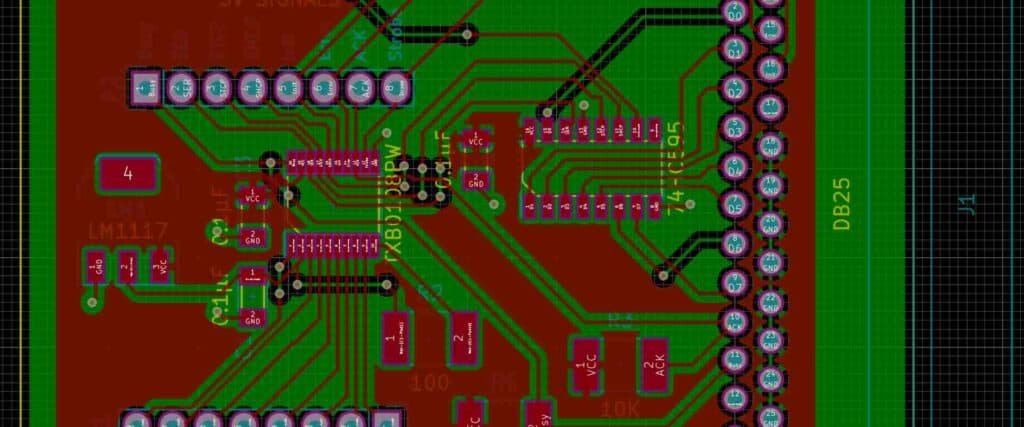
When designing a printed circuit board (PCB), it is essential to consider the trace design. A trace is a conductive path on the PCB that connects components. The trace design is crucial because it affects the performance and reliability of the PCB. Here are some factors to consider in trace PCB design:
Trace Width and Spacing
The width and spacing of traces affect the resistance, capacitance, and inductance of the PCB. A narrow trace has higher resistance and lower capacitance than a wide trace. A closely spaced trace has higher capacitance and lower inductance than a widely spaced trace. The trace width and spacing depend on the current and voltage requirements of the circuit. A high current or voltage requires a wider trace with more spacing.
Trace Length and Routing
The length and routing of traces affect the signal integrity and electromagnetic interference (EMI) of the PCB. A long trace has higher resistance, capacitance, and inductance than a short trace. A meandering trace has higher inductance and EMI than a straight trace. The trace length and routing depend on the signal frequency and impedance of the circuit. A high-frequency or high-impedance signal requires a shorter and straighter trace.
Trace Layer and Stackup
The layer and stackup of traces affect the signal routing and power distribution of the PCB. A single-layer PCB has limited routing options and power distribution. A multi-layer PCB has more routing options and power distribution, but also more complexity and cost. The trace layer and stackup depend on the size and complexity of the circuit. A small and simple circuit may use a single-layer PCB, while a large and complex circuit may use a multi-layer PCB.
Trace Material and Plating
The material and plating of traces affect the conductivity and corrosion resistance of the PCB. A copper trace has high conductivity and corrosion resistance, but also high cost and weight. A silver or gold trace has higher conductivity and corrosion resistance than copper, but also higher cost. The plating of traces affects the solderability and surface finish of the PCB. The trace material and plating depend on the performance and cost requirements of the circuit. A high-performance and high-reliability circuit may use silver or gold traces, while a low-cost and low-reliability circuit may use copper traces.
In summary, trace PCB design is a critical aspect of PCB design that affects the performance and reliability of the circuit. The trace width and spacing, length and routing, layer and stackup, and material and plating are the main factors to consider in trace PCB design. By optimizing these factors, you can achieve the desired performance and reliability of the circuit.
Trace Width and Spacing
Trace width and spacing are two important factors to consider when designing a printed circuit board (PCB). The width of a trace determines how much current it can carry without overheating, while the spacing between traces affects the overall size and complexity of the PCB.
When determining the appropriate trace width for a given circuit, it is important to consider the maximum current that will be flowing through the trace. The wider the trace, the more current it can carry without overheating. However, wider traces also take up more space on the PCB, which can be a limiting factor in designs with tight space constraints.
Spacing between traces is also an important consideration. In general, the closer together traces are, the more complex and compact the PCB design can be. However, if traces are too close together, it can lead to interference and crosstalk between signals. Therefore, it is important to strike a balance between trace spacing and PCB size.
To determine the appropriate trace width and spacing for a given design, it is important to consult industry standards and design guidelines. These guidelines take into account factors such as the maximum current, signal frequency, and overall PCB size to provide recommendations for trace width and spacing.
In summary, trace width and spacing are important factors to consider when designing a PCB. By carefully selecting the appropriate trace width and spacing for a given design, engineers can ensure that their PCBs are both reliable and efficient.
Trace Routing Techniques
Trace routing is an essential part of PCB design that involves the creation of a path for electrical signals to travel between components on a circuit board. Here are some common trace routing techniques used in PCB design:
1. Manhattan Routing
Manhattan routing is a simple and straightforward technique that involves creating 90-degree angles in the trace routing. This technique is commonly used in designs that have a high density of components and require precise routing.
2. Curved Routing
Curved routing is a technique that involves creating curves in the trace routing. This technique is commonly used in designs that require a smooth flow of signals and where space is not a constraint.
3. Meandering Routing
Meandering routing is a technique that involves creating a series of curves in the trace routing. This technique is commonly used in designs that require a longer trace length and where space is a constraint.
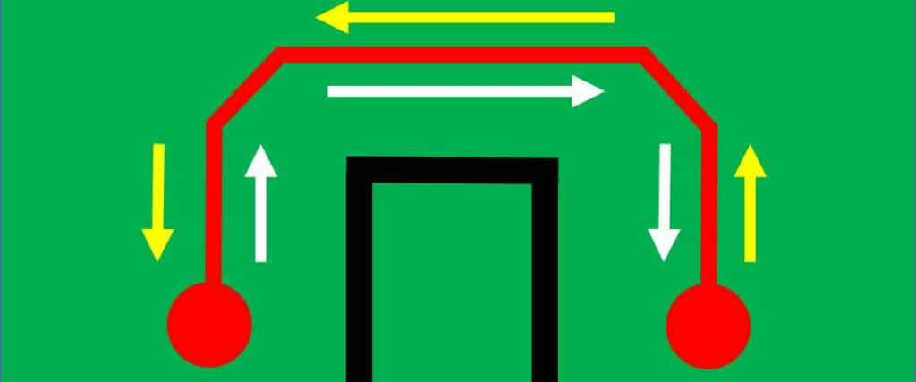
4. Differential Pair Routing
Differential pair routing is a technique that involves routing two traces parallel to each other. This technique is commonly used in designs that require high-speed data transmission and where signal integrity is critical.
5. Via Stitching
Via stitching is a technique that involves placing vias around a pad or component to provide a low-impedance path for signals. This technique is commonly used in designs that require high-speed data transmission and where signal integrity is critical.
In conclusion, trace routing is a critical part of PCB design that requires careful consideration of the design requirements and constraints. By using the appropriate trace routing techniques, designers can ensure that their designs meet the required performance and functionality.
Grounding and Power Distribution
When it comes to designing a trace PCB, proper grounding and power distribution are crucial for ensuring the reliability and performance of the circuit.
Grounding refers to the process of connecting all the ground points in the circuit together to create a common reference point for all the signals in the circuit. This is important because it helps to prevent noise and interference from affecting the signals in the circuit.
Power distribution, on the other hand, refers to the process of distributing power to all the components in the circuit. This is important because it helps to ensure that each component is receiving the correct amount of power, which is essential for proper functioning of the circuit.
To achieve proper grounding and power distribution, it is important to carefully plan the layout of the PCB. This includes placing the ground plane on the bottom layer of the board, and ensuring that all the ground connections are as short and direct as possible.
In addition, it is important to use proper decoupling techniques to reduce noise and interference in the circuit. This can be achieved by placing capacitors between the power and ground planes at regular intervals throughout the circuit.
Overall, proper grounding and power distribution are essential for the reliable and efficient operation of a trace PCB. By carefully planning the layout of the board and using proper decoupling techniques, designers can ensure that their circuits are free from noise and interference, and that each component is receiving the correct amount of power.
Signal Integrity and High-Speed Design Considerations
When designing a PCB for high-speed applications, signal integrity becomes a critical factor. Signal integrity refers to the ability of a signal to maintain its quality during transmission, and it is affected by various factors such as impedance, noise, and crosstalk.
One of the primary considerations for high-speed PCB design is the trace routing. The length, width, and spacing of the traces can significantly impact signal integrity. For instance, longer traces can result in higher signal attenuation, while narrower traces can increase impedance and cause signal reflections. Therefore, it is essential to choose appropriate trace widths and lengths based on the signal frequency and the PCB’s material properties.
Another critical aspect of high-speed design is the use of vias. Vias can introduce impedance discontinuities and cause signal reflections, which can degrade signal quality. Therefore, it is essential to minimize the number of vias and use them only when necessary. Additionally, it is crucial to use the right type of vias, such as blind vias or buried vias, based on the application’s requirements.
To ensure signal integrity, it is also crucial to consider the placement of components on the PCB. High-speed components such as microprocessors and memory chips should be placed close to each other to minimize trace lengths and reduce noise. Furthermore, it is essential to separate analog and digital components to prevent crosstalk and interference.
In conclusion, high-speed PCB design requires careful consideration of signal integrity and various other factors. By following best practices such as appropriate trace routing, minimizing vias, and careful component placement, designers can ensure that their PCBs meet the necessary performance requirements.
Testing and Validation
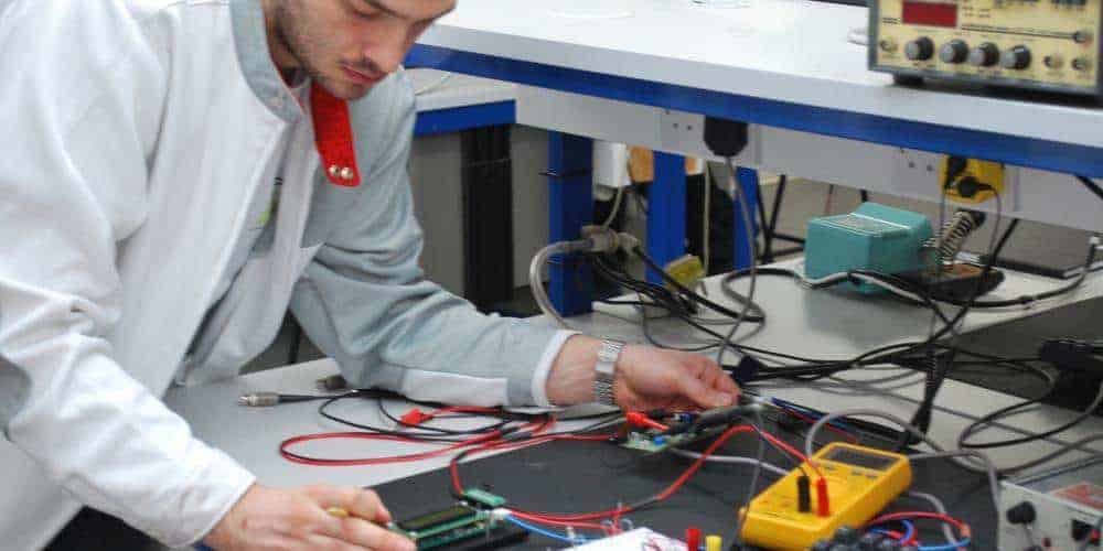
Once the PCB design is completed, it is essential to test and validate the design to ensure that it meets the required specifications. This step is crucial to ensure that the PCB functions as intended and that any potential issues are identified and corrected before the product is released to the market.
There are various methods of testing and validating a PCB design, including:
-
Design Rule Check (DRC): The DRC is a software tool that checks the design against a set of rules to ensure that it meets the required specifications. This step helps to identify any potential errors in the design, such as incorrect trace widths or spacing.
-
Electrical Rule Check (ERC): The ERC is a software tool that checks the design against a set of electrical rules to ensure that the circuit functions as intended. This step helps to identify any potential issues with the circuit, such as incorrect component values or incorrect connections.
-
Signal Integrity Analysis: Signal integrity analysis is a critical step in the testing and validation process. It helps to ensure that the signals on the PCB are of high quality and that the circuit functions as intended. This step involves analyzing the PCB’s electrical characteristics, such as impedance, capacitance, and inductance.
-
Prototype Testing: Once the design has been validated using software tools, it is essential to test the physical prototype to ensure that it functions as intended. This step involves testing the PCB’s electrical characteristics, such as voltage, current, and resistance.
In conclusion, testing and validation are essential steps in the PCB design process. By using software tools and prototype testing, designers can ensure that the design meets the required specifications and functions as intended.
