Wiring board design is a critical aspect of electronic device development. It involves designing the circuitry for printed circuit boards (PCBs) that are used in a wide range of electronic devices, from smartphones to medical equipment. The design process requires a deep understanding of electrical engineering principles, as well as knowledge of the latest design software and tools.
The goal of wiring board design is to create a circuit board that is efficient, reliable, and cost-effective. This involves carefully selecting the components that will be used on the board, as well as designing the layout of the circuitry in a way that minimizes interference and maximizes performance. Designers must also consider factors such as power consumption, heat dissipation, and signal integrity to ensure that the board will function properly in real-world conditions.
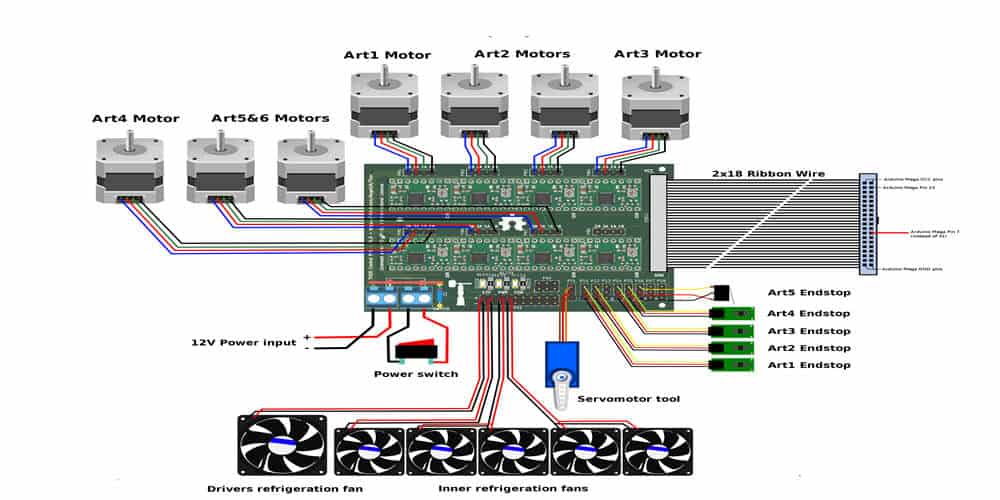
Basics of Wiring Board Design
Wiring board design is the process of creating a physical circuit board that will contain the various components needed for a particular electronic device. It involves the layout of the board, the placement of the components, and the routing of the electrical connections between them.
One of the most important considerations in wiring board design is the size and shape of the board itself. This will depend on the size and number of components that need to be included, as well as the overall size of the device that the board will be a part of. It is also important to consider the placement of any connectors or other external interfaces that the board will need to be connected to.
Another key factor in wiring board design is the placement of the components themselves. This will depend on a number of factors, including the size and shape of the components, their electrical characteristics, and their proximity to other components on the board. It is important to ensure that components are placed in such a way that they do not interfere with each other or with the routing of the electrical connections between them.
The routing of the electrical connections on the board is also a critical aspect of wiring board design. This involves determining the most efficient and effective way to connect the various components on the board, while minimizing the length of the connections and avoiding any potential interference or crosstalk between them. Techniques such as trace width optimization, via placement optimization, and layer stackup optimization can all be used to help optimize the routing of the board.
Overall, wiring board design is a complex and challenging process that requires careful attention to detail and a deep understanding of the underlying principles of electronics and circuit design. By following best practices and utilizing the latest tools and techniques, however, it is possible to create high-quality and reliable wiring boards that meet the needs of a wide range of electronic devices.
Key Components of Wiring Board Design

Wiring board design is an essential aspect of creating electronic devices. It involves the process of designing and manufacturing printed circuit boards (PCBs) that connect electronic components to each other. Here are some key components of wiring board design that you should consider.
Material Selection
The choice of material for wiring board design is critical. The most commonly used materials for PCBs are fiberglass and epoxy resin. These materials are preferred because they are durable, lightweight, and resistant to heat and moisture. Other materials used for wiring board design include ceramic, Teflon, and polyimide.
Trace Routing
Trace routing is the process of designing the paths that connect electronic components on a wiring board. The routing must be carefully planned to ensure that there is no interference between different components. The width, spacing, and length of the traces must be optimized to minimize signal loss and interference.
Component Placement
Component placement is another critical aspect of wiring board design. The placement of components must be optimized to minimize the length of the traces and reduce the risk of interference. The size and shape of the components must also be considered to ensure that they fit on the board and do not interfere with other components.
Ground Planes
Ground planes are large areas of copper that are connected to the ground. They help to reduce interference and noise by providing a low impedance path for electrical signals. Ground planes must be carefully designed to ensure that they are connected to all components that require a ground connection.
Power Planes
Power planes are similar to ground planes but are used to provide power to electronic components. They help to reduce noise and interference by providing a low impedance path for electrical signals. Power planes must be carefully designed to ensure that they can supply enough power to all components that require it.
In conclusion, wiring board design is a complex process that involves many different components. Material selection, trace routing, component placement, ground planes, and power planes are all critical aspects of wiring board design that must be carefully considered to ensure that the final product is reliable and functional.
Design Considerations for Wiring Board Design

When designing a wiring board, there are several key considerations that must be taken into account to ensure that the final product meets the required specifications and performs as expected. These considerations include:
1. Electrical Requirements
The first consideration when designing a wiring board is the electrical requirements. This includes the voltage, current, and frequency requirements of the circuit. It is important to ensure that the wiring board is designed to handle the required electrical load and that the components used are rated appropriately.
2. Layout and Placement
The layout and placement of components on the wiring board is another important consideration. The layout should be designed to minimize the length of the wiring and the number of vias required. This can help to reduce signal loss and improve the overall performance of the circuit.
3. Signal Integrity
Signal integrity is critical in high-speed circuits. It is important to ensure that the wiring board design takes into account the characteristic impedance of the traces, the length of the traces, and the termination of the signals. Failure to properly design for signal integrity can result in signal degradation and reduced performance.
4. Thermal Management
Thermal management is another important consideration in wiring board design. The design should incorporate appropriate thermal management techniques such as the use of heat sinks, thermal vias, and thermal pads to ensure that the components do not overheat and fail.
In summary, wiring board design requires careful consideration of electrical requirements, layout and placement, signal integrity, and thermal management. By taking these factors into account, designers can ensure that the final product meets the required specifications and performs as expected.
Testing and Validation for Wiring Board Design
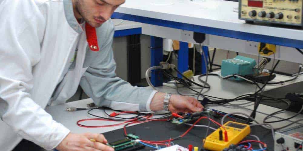
Testing and validation are crucial stages in the development of a wiring board design. They ensure that the board meets the required specifications and performs its intended functions. Testing and validation also help identify any potential issues or defects in the design that may need to be addressed before the board is released for production.
There are various methods of testing and validating a wiring board design, including:
-
Functional testing: This involves testing the board’s functionality by applying various input signals and verifying the corresponding output signals. Functional testing ensures that the board performs its intended functions as specified in the design requirements.
-
Electrical testing: This involves testing the board’s electrical characteristics, such as voltage, current, resistance, and capacitance. Electrical testing helps ensure that the board meets the required electrical specifications and operates within the specified limits.
-
Environmental testing: This involves testing the board’s performance under different environmental conditions, such as temperature, humidity, vibration, and shock. Environmental testing helps ensure that the board can withstand the expected operating conditions and maintain its performance over time.
-
Reliability testing: This involves testing the board’s reliability by subjecting it to various stress factors, such as accelerated aging, thermal cycling, and mechanical shock. Reliability testing helps ensure that the board can withstand the expected operating conditions and maintain its performance over its expected lifespan.
In addition to these testing methods, validation also involves verifying the board’s compliance with industry standards and regulations, such as IPC-A-600 and RoHS.
Overall, testing and validation are critical stages in the development of a wiring board design. They help ensure that the board meets the required specifications, performs its intended functions, and can withstand the expected operating conditions. By following these testing and validation procedures, designers can ensure that their wiring board designs are reliable, efficient, and safe for use.
