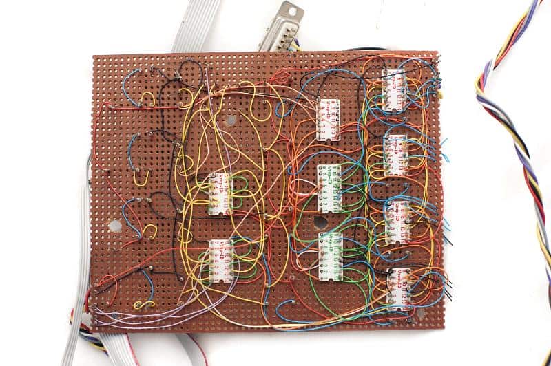
Wiring boards are used in electronic circuits and devices. The printed wiring board, or PCB, was introduced in the early 1950s. Its main purpose is to increase the number of electronic components per square inch and reduce board size without affecting circuit performance. Its advantages over traditional circuit boards include increased component density and flexibility, making it easier to assemble and test.
We can manufacture printed wiring boards using different methods. For instance, a reverse-engineering process called CAD/CAM can help create circuit traces with a smaller hole size than traditional methods. This can result in shorter processing times and reduced tooling costs. In addition, we can also automate the process, which increases the production rate and lowers labor costs.
Another method of assembling circuit boards is by using flex circuit boards. These flexible boards can bend, fold, and wrap around various objects. Their flexibility allows them to help in applications that are impossible with traditional flat circuit boards. Additionally, they can fold at an angle and still carry current.
Routing and assembling circuit boards can be automated using CAD tools. In addition, it includes features that allow you to create manufacturing drawings and output files.
What is the Standard Size of a Wiring Board?
There are several dimensions to consider when calculating the standard size of a wiring board. These dimensions include pad spacing, trace spacing, and copper trace width. Generally, these dimensions must be within a specific range, usually 0.003 to 0.010 inches. In addition, copper trace width and spacing are essential for EMI/EMC considerations.
Dimensions
When choosing a wiring board, it is important to consider its dimensions. The PCB’s copper weight is an important dimension to take into consideration. Copper weight refers to the thickness of the copper tracks that comprise the board. Standard options are 0.5 oz (17.5 um), 1.0 oz (35 um) or 2.0 oz (70 um). The greater the copper weight, the lower the track resistance.
Materials
Choosing the right materials for your wiring board is essential for safe and efficient performance. Copper wire is the best choice for home use, as it is less prone to corrosion. Aluminum wire is a less expensive alternative but is not as conductive as copper. When buying wire, look for a manufacturer that adheres to the highest industry standards.
Wire comes in solid and stranded varieties. Solid wire is made of a single metal wire strand, while the stranded wire consists of several smaller pieces. Solid wire is generally less flexible than stranded wire, which makes it more pliable. You can choose between solid and stranded wire by reading the markings on the wire.
Solder mask
The solder mask size of a wiring board is an essential aspect of soldering electronic components. Its job is to cover copper traces in a circuit board. Various materials can create solder masks, and each mask size has its specific application.
Before applying solder mask ink, we need to prepare a clean board. The coating thickness varies according to the reliability requirements of the circuit board. It also differs depending on the area of the board. An experienced PCB manufacturer will specify a solder mask thickness for each board.
The solder mask, also known as solder resist, is a thin layer of polymer that covers copper traces to prevent oxidation and contamination. It also minimizes the risk of solder bridges between pads. A solder bridge connects two conducting parts of a board by whisking the solder. The solder mask plays a critical role in mass-produced circuit boards. It helps ensure that solder is applied correctly.
Moreover, solder masks come in a variety of colors. Some are red, and others are blue. Red solder masks are often used for aesthetic purposes, providing a striking contrast. Green and blue solder masks are also available and used in electronics production.
Drill hole specifications
When drilling holes in a wiring board, the diameter of the hole must be a specific size. It must not be larger than 0.0135″ in diameter. There are two kinds of holes for PCBs: via holes and non-via holes. Via holes are used for current flow between two board layers, while we use non-via holes for component insertion.
Drill hole specifications for PCBs depend on the standard and the size of the electrical components used. For example, a 0.5mm component requires a hole that is 0.8mm in diameter. The DSS and SSS specifications specify that the hole size must be 0.3mm wider than the component’s diameter.
The size of a hole is another factor that affects the overall cost of a PCB. It also affects the performance of the board. Drill holes that are too small or too large will add to the cost of the board. In addition, they can make a PCB more challenging to assemble.
Drill hole specifications for the wiring board are an essential design step. With proper planning, you can avoid mistakes and achieve a professional-looking design. In addition, the right design software will allow you to customize yours via sizes and tooling hole features. A program like Altium designer provides advanced CAD tools to build the highest quality layouts. It also has features that help you optimize nets and trace clearance. It can even route between layers.

Thieving a wiring board
Thieving a wiring board is adding copper to the board from areas where it is not needed. This wiring board is essential in maintaining a uniform copper distribution throughout aboard. This prevents uneven plating and deformation, reducing the structural integrity. Thieving can also avoid over-plating or etching in certain board areas. However, these practices can add unnecessary costs to a project, so following some guidelines is essential.
Generally, thieving will appear as a diamond or dot pattern on the PCB. This results from a manufacturing process that will not attach to a net. This isn’t the best idea from an EMC standpoint, so you should attach the thieving yourself to a net that does have a ground net.
You can make the process more manageable if you use a thieving tool. This device includes a solder pad with an annular shape around a through-hole 33. The pad also has a thin bridge 34 connecting it to the thieving pad 36. We etch these elements from a copper-coated PWB.
Another method of copper thieving is adding dummy copper pads to a PCB. We plate copper over the board’s surface with small copper squares and dots during this process. This ensures that the copper plating is uniform throughout the board and the copper in the holes is more consistent.
