HDILayout is a term used to describe the layout of a website or application that is designed to be user-friendly and easy to navigate. The purpose of HDILayout is to create a seamless experience for the user, allowing them to quickly and easily find what they are looking for. This is achieved through the use of clear and concise navigation, intuitive design, and a focus on user experience.
One of the key features of HDILayout is its focus on simplicity. The layout is designed to be easy to understand and navigate, with a clear hierarchy of information that guides the user through the site or application. This is achieved through the use of clear headings, intuitive icons, and a consistent design throughout the site.
Another important aspect of HDILayout is its focus on accessibility. The layout is designed to be accessible to users of all abilities, including those with visual impairments or other disabilities. This is achieved through the use of clear and easy-to-read fonts, high contrast colors, and other design features that make the site or application easy to use for everyone.
What is HDI Layout?
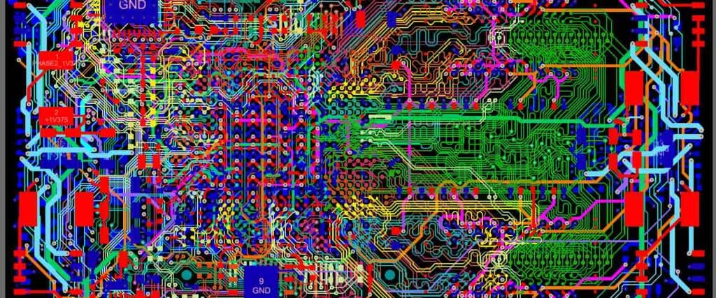
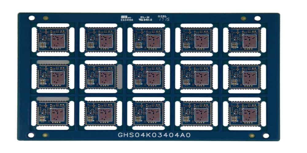
HDI (High-Density Interconnect) layout is a printed circuit board (PCB) design technique that allows for a high density of components to be placed on a small area of the board. This technique is commonly used in electronic devices where space is at a premium, such as smartphones, tablets, and other portable devices.
The HDI layout technique uses microvias, which are small holes drilled into the PCB that connect layers of the board. These microvias allow for a higher density of components to be placed on the board, as they take up less space than traditional through-hole vias.
HDI layout also allows for the use of smaller components, such as microchips and surface mount devices (SMDs), which can be placed closer together on the board. This results in a more compact and efficient design.
In addition to its space-saving benefits, HDI layout can also improve the electrical performance of the PCB. The shorter traces and reduced signal interference between components can result in faster signal transmission and reduced noise.
Overall, HDI layout is a valuable technique for designing compact and high-performance PCBs for a variety of electronic devices.
The Importance of HDI Layout
HDI (High-Density Interconnect) Layout is a crucial aspect of modern printed circuit board (PCB) design. It involves using advanced techniques to create densely packed, complex circuit boards that offer high performance and reliability. Here are a few reasons why HDI layout is so important:
1. Space Saving
HDI layout allows designers to pack more components onto a smaller board, which is essential in applications where space is at a premium. This is achieved through the use of advanced routing techniques, such as microvias, blind vias, and buried vias, which allow for more efficient use of the available space.
2. High-Speed Performance
HDI layout is also critical for achieving high-speed performance in modern PCBs. By minimizing the length of signal paths and reducing the number of vias, designers can reduce signal loss and improve signal integrity. This is particularly important in applications where high-frequency signals are used, such as in telecommunications, data centers, and aerospace.
3. Improved Reliability
Finally, HDI layout can also improve the reliability of PCBs. By reducing the number of vias and optimizing the routing of signal paths, designers can minimize the risk of signal interference, crosstalk, and other issues that can compromise the performance of a circuit board. This can result in higher product yields, lower failure rates, and reduced costs.
In summary, HDI layout is an essential aspect of modern PCB design that offers numerous benefits, including space saving, high-speed performance, and improved reliability. By using advanced routing techniques and design tools, designers can create complex, densely packed circuit boards that meet the demands of today’s high-tech applications.
Factors to Consider in HDI Layout
When designing a High-Density Interconnect (HDI) layout, there are several factors that must be taken into consideration to ensure the optimal functionality of the final product. These factors include:
1. Signal Integrity
Signal integrity is one of the most critical factors to consider in HDI layout design. The layout should be designed in such a way that it minimizes signal noise, crosstalk, and electromagnetic interference (EMI). This can be achieved by using proper grounding, power supply, and signal routing techniques.
2. Thermal Management
HDI layouts tend to generate a lot of heat due to the high-density of components. Therefore, it is essential to consider thermal management techniques during the design process. This includes using thermal vias, thermal pads, and heat sinks to dissipate heat effectively.
3. Manufacturing Constraints
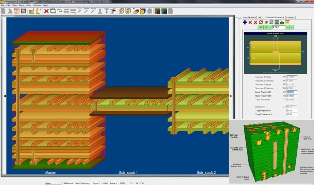
HDI layouts are complex and require specialized manufacturing techniques. Therefore, it is essential to consider the manufacturing constraints during the design process. This includes selecting the right materials, choosing the appropriate board thickness, and ensuring that the layout is manufacturable.
4. Component Placement
The placement of components is crucial in HDI layout design. Components should be placed in such a way that they do not interfere with each other and that they are easily accessible for testing and maintenance. This can be achieved by using proper component spacing, orientation, and placement rules.
5. Cost
HDI layouts are more expensive to manufacture than traditional PCB layouts due to their complexity. Therefore, it is essential to consider the cost implications during the design process. This includes selecting the right materials, minimizing the number of layers, and optimizing the layout to reduce manufacturing costs.
In conclusion, the factors mentioned above are critical to consider when designing an HDI layout. By taking these factors into account, designers can ensure that the final product is reliable, efficient, and cost-effective.
Designing HDI Layouts
High-Density Interconnect (HDI) is a type of printed circuit board (PCB) technology that allows for the creation of smaller, more complex electronic devices. HDI layouts are designed to maximize the use of space on a PCB and to increase the number of electrical connections that can be made between components. Here are some tips for designing effective HDI layouts:
-
Start with a clear plan: Before designing an HDI layout, it’s important to have a clear plan for the device you’re creating. This includes understanding the size and shape of the PCB, the number and placement of components, and the electrical requirements of the device.
-
Choose the right materials: HDI layouts require special materials, such as thin dielectric layers, to create the necessary connections between components. It’s important to choose materials that are compatible with the components you’re using and that can withstand the environmental conditions the device will be exposed to.
-
Use microvias: Microvias are small holes drilled into the PCB that allow for the creation of more connections in a smaller space. Using microvias can help you create a more compact and efficient HDI layout.
-
Consider component placement: The placement of components on an HDI layout is critical to its success. Components should be placed in a way that maximizes the use of space on the PCB and that allows for efficient routing of electrical connections.
-
Pay attention to signal integrity: HDI layouts can be more prone to signal integrity issues, such as noise and interference, than traditional PCB layouts. It’s important to pay close attention to signal integrity when designing an HDI layout to ensure that the device functions as intended.
Overall, designing an effective HDI layout requires careful planning, attention to detail, and an understanding of the unique challenges and opportunities presented by this technology. By following these tips and working with experienced PCB designers, you can create high-quality HDI layouts that meet your device’s needs.
Best Practices for HDI Layouts
When designing an HDI (High-Density Interconnect) layout, there are several best practices to keep in mind to ensure optimal performance and reliability. Here are some key considerations to keep in mind:
-
Minimize the number of vias: The more vias there are in an HDI layout, the higher the risk of signal integrity issues and manufacturing defects. Therefore, it’s important to minimize the number of vias as much as possible while still meeting the design requirements. One way to do this is to use blind or buried vias instead of through-hole vias, as they take up less space and reduce the number of required layers.
-
Use appropriate trace widths and spacing: The trace widths and spacing in an HDI layout should be carefully selected to ensure that they can handle the required current and voltage levels without causing signal interference or crosstalk. In general, wider traces can handle more current, while narrower traces can be used to save space. The spacing between traces should be large enough to prevent electrical coupling between adjacent signals.
-
Keep signal paths as short as possible: In an HDI layout, signal paths can be very complex and convoluted, which can lead to signal degradation and interference. To minimize these issues, it’s important to keep signal paths as short and direct as possible. This can be achieved by using optimized routing algorithms and carefully selecting the location of components.
-
Avoid sharp corners and acute angles: Sharp corners and acute angles in an HDI layout can lead to manufacturing defects and reliability issues. Therefore, it’s important to avoid them as much as possible. Instead, use rounded corners and gentle angles to ensure that the layout is manufacturable and reliable.
-
Ensure proper grounding and shielding: In an HDI layout, proper grounding and shielding are essential to prevent signal interference and crosstalk. Therefore, it’s important to ensure that all signal and power planes are properly grounded and shielded, and that there are no ground loops or other grounding issues that could cause problems.
By following these best practices, you can ensure that your HDI layout is optimized for performance, reliability, and manufacturability.
