The advent of multilayer PCBs has contributed to the production several electronic devices. Multilayer circuit boards are a better option for high performance devices. This is because these boards provide improved signal routing and better shielding. Also, there are more layouts for this PCB design. Compared to dual layer or single layer boards, these boards offer more density for routing signal and power tracks.
Designing a multilayer PCB prototype is required before commencing with large scale PCB manufacturing runs. Here, we will be discussing multilayer PB prototype and their benefits in multilayer printed circuit board production.
What is a Multilayer PCB?
A multilayer PCB is a type of printed circuit board that comprises more than two conductive layers of copper. This circuit board has at least three conductive layers. For a multilayer board, the bottom and top layers are similar to that of a dual layer PCB. However, a multilayer board comprises more layers on the two sides of the core.
Also, copper plated holes create interconnection between these multiple layers. Multilayer PCBs can have up to 40 layers. The passive and active components of this board are usually mounted on the bottom and top layers of the multiple layer board. Furthermore, the inner layers of the circuit board are specially designed for routing.
Multilayer PCB board comprises more electronic components which make it ideal for use in modern-day electronic devices. Smart devices always need between four to eight layers. For instance, smartphones will need about twelve layers. Multilayer PCB manufacturing requires designers to select an even number of layers. This is because integrating odd number of layers can make PCB layout complex and can lead to high cost.
It is crucial to place signal layers close to planes in a four layer PCB stackup. This helps to enhance electromagnetic compatibility. Also, ground plane and signal trace often minimize plane impedance which reduces radiation from the cables linked to the PCB. The layers on a multilayer board help to distribute power.
PCB multilayer boards have multiple layers that require a good stackup. The stackup of a multilayer PCB board plays a significant role in its functionality. Also, multilayer PCBs have several layers which help to enhance their functionality in applications. Furthermore, multilayer PCBs have exceptional electrical characteristics.
What is a Multilayer PCB Prototype?
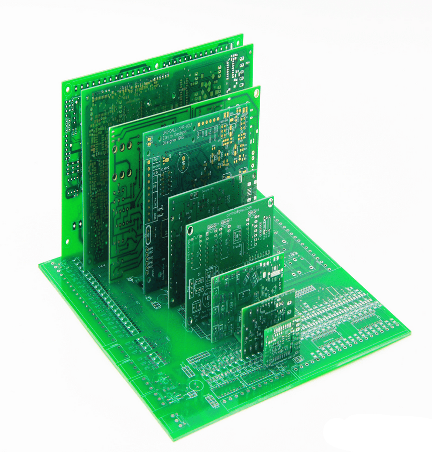
Multilayer PCB prototype is a sample of multilayer PCBs designed with the main purpose of testing its functionality. Prototypes help to evaluate basic user functionality. Engineers need functional multilayer PCB prototypes to evaluate the whole functionality of PCB designs.
Multilayer PCB board prototype is a step in the design process of a multilayer printed circuit board. PCBs integrate conductive tracks to create connection between components. Also, multilayer PCB prototype serves as a proof of concept. Multilayer PCB manufacturing is a complex process. Therefore, it is crucial to verify the functionality of this board before commencing a full production run.
Small errors can affect the functionality of the final PCB. Also, the failure to detect these problems before a full production run can result in high PCB manufacturing cost. Therefore, engineers request for a multilayer PCB prototype before full scale PCB manufacturing.
In addition, the multilayer PCB prototype is essential throughout the design process. Prototyping requires testing the functionality of the PCB idea with every new change or addition. Also, this process enabled designers to test the PCB at multiple phases of the design and make any corrections as required.
Also, multilayer PCB prototype comprises the required functions and features of the final PCB product. Therefore, prototyping helps to detect the problems or defects in the design.
Why is Multilayer PCB Prototype Important?
Generally speaking, prototypes are crucial in PCB manufacturig. These multilayer PCB prototypes are usually created to detect any flaw in multiple stages of PCB manufacturing. Multilayer PCB manufacturing process is a complex one that requires more efforts and resources. Therefore, it is crucial to detect errors early enough so as to prevent spending too much on PCB manufacturing.
Early detection of errors
One of the major purposes of carrying out multilayer PCB board prototype is to evaluate the functionality of a board. Therefore, this helps to detect possible errors in the multilayer PCBs. Also, if there is a faulty board, prototyping will help to detect the defect before beginning large scale production.
Minimized PCB manufacturing cost
When a faulty PCB goes into a full production run, it will take more money to fix the problems. In some cases, the PCB manufacturer may need to fabricate a new PCB depending on the nature of the problem. With design testing and early detection of problems, you can reduce the cost of PCB manufacturing.
Reduced timeline
Multilayer PCB prototype helps to reduce the time spent on PCB manufacturing. It takes more time to fix a problem in a PCB if it is already in the PCB manufacturing stage. However, you can reduce PCB manufacturing time when a problem has been detected and fixed during the design stage.
Components testing
Also, multilayer PCB prototype allows you to test components individually. It enables PCB designers to test individual functions and components.
How do Multilayer Boards Work?
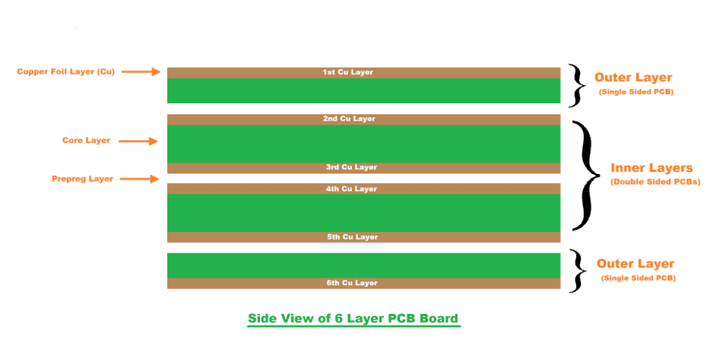
The first step in multilayer PCB manufacturing is designing the PCB layout. After the PCB design, you need to build the laminate and inner layer core. The next step involves laminating the inner layer core, copper foil sheets, and the prepreg sheets. Also, the lamination process involves the use of heat and pressure to bond the layers. While doing this, ensure there is no air trapped in the layers.
Furthermore, a multilayer PCB features a power plane and ground plane. Also, the power layers are often in the middle of the printed circuit board while the ground layer is very close to the top layer. There is space for signal tracks once the PCB designer has built the inner layers.
A multilayer PCB features so many layers. Therefore, the stackup of a multilayer PCB is very crucial. For a multilayer printed circuit boards, it is better to have an even number of layers. Multilayer PCBs function well by combining alternating layers of core materials and prepreg in a unit. Therefore, these board manufacturing integrate high pressure and heat for uniform encapsulation.
Multilayer PCBs have multiple layers of material and as such, there must be proper drilling of holes among layers.
Conclusion
The demand for multilayer PCBs is very high. Multilayer PCBs are crucial in the production of technology devices, military equipment, and consumer products among others. Also, multilayer PCBs offer great benefits. However, the fabrication of multilayer PCBs is a complex process that involves several steps. Therefore, it is crucial to avoid errors during the production of multilayer PCBs. Multilayer PCBs prototypes are important before commencing with the final production of these boards.
