PCB filter design is an integral part of electronic circuit design. PCB filters are used to remove unwanted signals and noise from electronic circuits. They are designed to attenuate signals at specific frequencies, while allowing desired signals to pass through. PCB filters are used in a wide range of electronic devices, including radios, televisions, and computers.
There are several types of PCB filters, including low-pass, high-pass, band-pass, and band-stop filters. Each type of filter is designed to attenuate signals at specific frequencies. Low-pass filters attenuate high-frequency signals, while allowing low-frequency signals to pass through. High-pass filters do the opposite, attenuating low-frequency signals and allowing high-frequency signals to pass through. Band-pass filters attenuate signals outside of a specific frequency range, while allowing signals within that range to pass through. Band-stop filters do the opposite, attenuating signals within a specific frequency range and allowing signals outside of that range to pass through.
PCB filter design is a complex process that requires a deep understanding of circuit theory and signal processing. Designers must take into account the frequency response of the filter, as well as the impedance of the circuit and the desired cutoff frequency. They must also consider the physical layout of the filter on the PCB, as well as the size and type of components used. Despite the complexity of the process, PCB filter design is essential for ensuring the proper functioning of electronic circuits.
Basic Concepts
PCB filter design is an important aspect of electronics design. It involves designing filters that can remove unwanted signals or noise from a circuit. The basic concept of a filter is to allow certain frequencies to pass through while blocking others. There are different types of filters, including low-pass, high-pass, band-pass, and band-stop filters.
The design of a filter depends on the specific application and the desired frequency response. A filter can be designed using passive components such as resistors, capacitors, and inductors, or active components such as operational amplifiers. The choice of components depends on factors such as cost, size, and performance requirements.
One important concept in filter design is the cutoff frequency, which is the frequency at which the filter starts to attenuate the signal. The cutoff frequency can be adjusted by changing the values of the components in the filter. Another important concept is the Q factor, which is a measure of the selectivity of the filter. A higher Q factor means a narrower bandwidth and a more selective filter.
In addition to passive and active components, PCB filter design may also involve the use of transmission lines, which can be used to create high-frequency filters. Transmission lines can be designed to have specific impedance values, which can be used to match the impedance of the filter to the impedance of the circuit.
Overall, PCB filter design is a complex and important aspect of electronics design. It requires a good understanding of the basic concepts and the ability to choose the right components and design the filter to meet the specific requirements of the application.
Filter Design Process
When designing a PCB filter, it is important to follow a systematic process to ensure that the filter meets the required specifications. The filter design process can be broken down into three main stages: specifications, topology selection, and component selection.
Specifications
The first step in the filter design process is to determine the specifications of the filter. This involves identifying the frequency range that needs to be filtered, the desired insertion loss, and the impedance of the input and output ports. Other important specifications may include the size and cost of the filter, as well as any environmental factors that may affect its performance.
Topology Selection
Once the specifications have been identified, the next step is to select a filter topology that will meet those specifications. There are many different types of filter topologies to choose from, including low-pass, high-pass, band-pass, and band-stop filters. The choice of topology will depend on the specific requirements of the application.
Component Selection
After the topology has been selected, the next step is to choose the appropriate components for the filter. This may involve selecting the values of resistors, capacitors, and inductors, as well as choosing the appropriate type of filter substrate and the number of layers required for the PCB. The choice of components will depend on the specific requirements of the filter topology and the application.
By following this systematic process, it is possible to design a PCB filter that meets the required specifications and performs optimally in the target application.
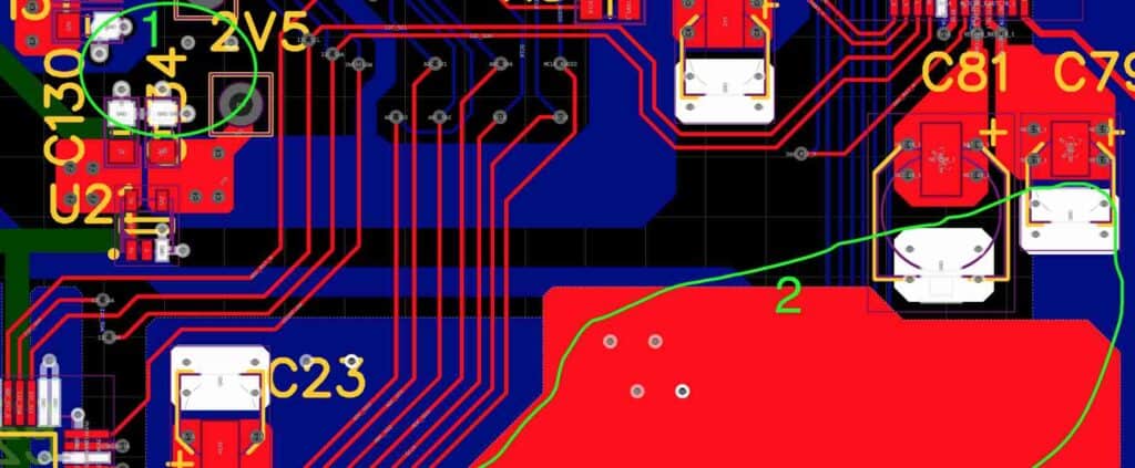
PCB Layout Design

When designing a PCB filter, the layout design is a crucial step that can significantly impact the filter’s performance. Proper PCB layout design ensures proper grounding and shielding, correct trace width and spacing, and optimal component placement.
Grounding and Shielding
Grounding and shielding are essential for reducing noise and interference in the filter circuit. Ground planes should be placed on both sides of the PCB, and all components should be connected to these planes. Additionally, shielding can be added to the filter circuit to further reduce noise and interference.
Trace Width and Spacing
Trace width and spacing are critical for minimizing losses and ensuring proper signal transmission. The trace width should be selected based on the current carrying capacity of the trace, and the spacing between traces should be sufficient to prevent crosstalk and interference.
Component Placement
Component placement is crucial for optimizing the filter’s performance. Components should be placed as close to each other as possible to minimize the trace length between them. Additionally, the placement of components should be carefully considered to ensure proper signal flow and minimize noise and interference.
In summary, proper PCB layout design is essential for the optimal performance of a PCB filter. Grounding and shielding, trace width and spacing, and component placement are all critical factors that must be carefully considered during the design process.
Simulation and Testing
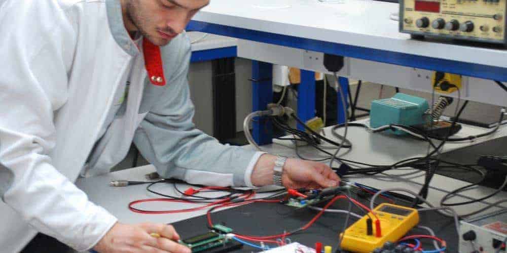
Once the PCB filter design is complete, it is essential to simulate and test the filter to ensure that it meets the desired specifications. Simulation and testing are crucial steps in the design process as they help to identify any issues or problems that may arise before the filter goes into production.
One of the most common simulation tools used for PCB filter design is SPICE (Simulation Program with Integrated Circuit Emphasis). SPICE allows designers to simulate the behavior of the filter under various conditions and helps to identify any potential issues with the design.
In addition to simulation, testing is also an important step in the design process. Testing involves measuring the performance of the filter under real-world conditions and comparing the results to the desired specifications. This can be done using specialized testing equipment, such as a network analyzer, which can measure the filter’s frequency response, insertion loss, and return loss.
During testing, it is essential to ensure that the filter meets all the desired specifications. If any issues are identified, the design can be modified and retested until the desired performance is achieved.
It is important to note that simulation and testing are not foolproof, and there may be some discrepancies between the simulated and actual performance of the filter. However, by using simulation and testing, designers can minimize the risk of issues arising during production and ensure that the filter meets the desired specifications.
In conclusion, simulation and testing are critical steps in PCB filter design. By using these tools, designers can identify and resolve any issues before the filter goes into production, ensuring that the filter meets the desired specifications.
Advanced Techniques
When it comes to designing PCB filters, there are several advanced techniques that can be employed to achieve better performance. Here are some of the most effective techniques:
1. Multiple Sections
One way to improve filter performance is to use multiple sections. By using multiple sections, it is possible to achieve a steeper roll-off and better stop-band attenuation. This technique is especially useful for filters with high-order responses.
2. Coupled Resonators
Another advanced technique is to use coupled resonators. Coupled resonators can be used to achieve a narrow bandwidth and high selectivity. This technique is often used in the design of bandpass filters.
3. Interdigital Filters
Interdigital filters are another advanced technique that can be used to achieve high selectivity and low insertion loss. These filters are constructed by interdigitating two sets of conductors on a substrate. Interdigital filters are often used in the design of microwave filters.
4. Elliptic Filters
Elliptic filters are a type of filter that can be used to achieve a sharp transition between the pass-band and stop-band. These filters have a very steep roll-off and provide excellent stop-band attenuation. However, they can be difficult to design and require a high degree of precision.
5. Distributed Filters
Distributed filters are another advanced technique that can be used to achieve high performance. These filters are constructed using transmission lines and can provide excellent performance at high frequencies. However, they can be difficult to design and require a good understanding of transmission line theory.
Overall, these advanced techniques can be used to achieve better performance from PCB filters. By employing these techniques, it is possible to achieve a steeper roll-off, better stop-band attenuation, and higher selectivity.
