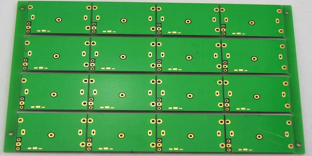
A 4 layer PCB board is a printed circuit board that consists of four layers of conductive material. It is widely used in electronic devices that require high performance and reliability. The four layers of the board are connected by vias, which are small holes that allow electrical signals to pass through the layers.
The use of a 4 layer PCB board has several advantages over a 2 layer board. Firstly, it provides more space for routing traces, which reduces the chances of signal interference and improves signal integrity. Secondly, it allows for more components to be placed on the board, which can increase the functionality of the device. Finally, it provides better thermal management, which can improve the overall performance and lifespan of the device.
What is a 4 Layer PCB Board?
A Printed Circuit Board (PCB) is an essential component of electronic devices, acting as a foundation for the connection of electronic components. A 4 Layer PCB Board is a type of PCB that has four layers of conductive material separated by insulating layers.
The four layers of conductive material allow for a more complex circuit design and provide more space for components. The additional layers also help to reduce electromagnetic interference and crosstalk between components, leading to a more reliable and efficient circuit.
Compared to a 2 Layer PCB Board, a 4 Layer PCB Board offers a higher level of complexity and flexibility in circuit design, making it a popular choice for more advanced electronic devices such as smartphones, computers, and medical equipment.
Designing and manufacturing a 4 Layer PCB Board requires specialized skills and equipment, making it a more expensive option than a 2 Layer PCB Board. However, the benefits of a 4 Layer PCB Board can outweigh the cost for certain applications, especially those that require a high level of reliability and performance.
In summary, a 4 Layer PCB Board is a type of PCB that has four layers of conductive material separated by insulating layers, providing more space for components and reducing electromagnetic interference. It is a popular choice for advanced electronic devices that require a higher level of complexity and flexibility in circuit design.
Advantages of 4 Layer PCB Boards
4 Layer PCB boards are becoming increasingly popular in the electronics industry due to their numerous advantages over other types of PCBs. Here are some of the key benefits of using a 4 Layer PCB board:
1. Increased Flexibility and Design Capabilities
A 4 Layer PCB board provides more layers for routing signals and power, which allows for greater flexibility in terms of design. This means that designers have more options when it comes to placing components and routing traces. With more layers, designers can create more complex circuits with less interference between components.
2. Improved Signal Integrity
With a 4 Layer PCB board, signals can be routed in a more controlled and efficient manner. This results in better signal integrity, which means that the signals are less likely to be distorted or degraded as they travel through the board. This is particularly important for high-speed digital circuits, where even small amounts of distortion can cause errors.
3. Higher Density and Smaller Size
Because a 4 Layer PCB board provides more layers for routing signals and power, it allows for higher density circuits in a smaller size. This is particularly useful in applications where space is limited, such as in mobile devices or wearables.
4. Improved Thermal Management
A 4 Layer PCB board can also help with thermal management. By having more layers, designers can create thicker copper planes which can dissipate heat more effectively. This is particularly important for power electronics, where heat dissipation is critical for the longevity of the components.
In conclusion, 4 Layer PCB boards offer numerous advantages over other types of PCBs. They provide increased flexibility and design capabilities, improved signal integrity, higher density and smaller size, and improved thermal management. These benefits make them an excellent choice for a wide range of applications in the electronics industry.
Design Considerations for 4 Layer PCB Boards

When designing 4 layer PCB boards, there are several considerations that should be taken into account to ensure optimal performance and functionality. Here are some key design considerations:
1. Layer stackup
The layer stackup of a 4 layer PCB board is critical for its performance. The stackup determines the order in which the layers are arranged, the thickness of each layer, and the type of material used. Some common stackups for 4 layer PCB boards include signal-ground-power-signal (SGPS) and signal-power-ground-signal (SPGS). The choice of stackup will depend on the specific requirements of the application.
2. Trace routing
Trace routing is another important consideration when designing 4 layer PCB boards. It is important to ensure that traces are routed in a way that minimizes noise, crosstalk, and interference. Some best practices for trace routing include keeping traces as short as possible, avoiding sharp corners, and minimizing the number of vias.
3. Power and ground planes
Power and ground planes are critical for ensuring proper power distribution and signal integrity in 4 layer PCB boards. It is important to ensure that these planes are properly connected and that there are no gaps or voids in the planes. Some best practices for power and ground planes include using a solid plane for each layer, minimizing the distance between the planes, and adding decoupling capacitors.
4. Component placement
Component placement is also important for ensuring optimal performance and functionality of 4 layer PCB boards. It is important to ensure that components are placed in a way that minimizes noise and interference. Some best practices for component placement include keeping sensitive components away from noisy components, keeping high-speed components close together, and minimizing the distance between components and their corresponding decoupling capacitors.
In summary, designing 4 layer PCB boards requires careful consideration of layer stackup, trace routing, power and ground planes, and component placement. By following best practices in each of these areas, designers can ensure optimal performance and functionality of their PCB boards.
Manufacturing Process for 4 Layer PCB Boards
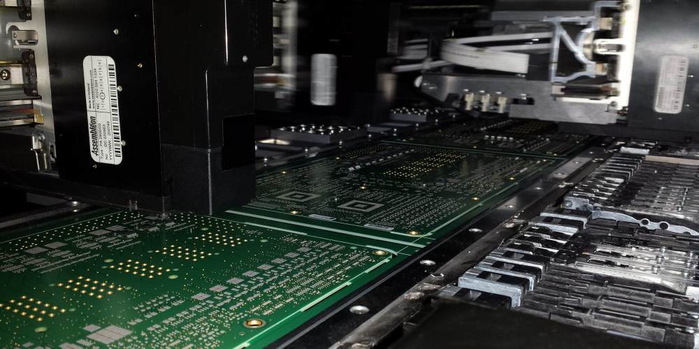
The manufacturing process for 4 layer PCB boards is a complex and intricate process that requires precision and attention to detail. The process involves several steps, including designing the PCB layout, drilling, plating, etching, and soldering.
Firstly, a design is created for the PCB layout using computer-aided design (CAD) software. The layout includes the placement of components and the routing of the traces on the board. Once the layout is finalized, it is printed on a special film called the photomask.
Next, the board is drilled using a CNC machine to create the holes for the components. The holes are then plated with a thin layer of copper to create a conductive path between the layers.
After the plating process, the board is etched using a chemical solution to remove the unwanted copper from the board. This process creates the necessary traces and pads on the board.
Finally, the board is soldered to attach the components. The soldering process involves heating the board and the components to a specific temperature to melt the solder and create a strong bond.
In conclusion, the manufacturing process for 4 layer PCB boards is a complex and precise process that involves several steps. The process requires attention to detail and precision to ensure that the final product is of high quality and meets the required specifications.
Testing and Quality Control for 4 Layer PCB Boards
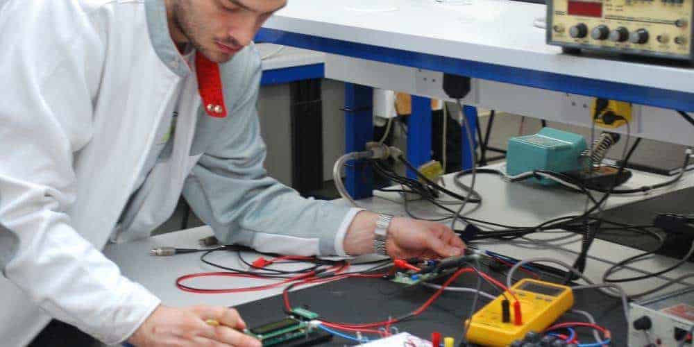
Testing and quality control are critical aspects of the 4 layer PCB board manufacturing process. It ensures that the board meets the required specifications and functions as intended. Here are some of the testing and quality control measures that are implemented during the manufacturing process.
Electrical Testing
Electrical testing is the most crucial aspect of PCB board testing. It involves checking the electrical connectivity of the board using various methods. The most common method is the automated optical inspection (AOI) method, which uses a camera to detect defects such as shorts and opens.
Another method is the flying probe test, which uses a series of probes to test the board’s electrical connectivity. This test is more accurate than the AOI method but takes longer to complete.
Visual Inspection
Visual inspection is another critical aspect of quality control. It involves checking the board’s physical appearance, such as its surface finish, solder mask, and silkscreen. The inspection ensures that the board meets the required standards and is free from any defects.
X-ray Inspection
X-ray inspection is used to detect defects that cannot be seen through visual inspection. It involves passing X-rays through the board to detect any hidden defects such as voids in the solder joints and misalignments.
Functionality Testing
Functionality testing ensures that the board meets its intended purpose. It involves testing the board’s performance under various conditions to ensure that it meets the required specifications.
In conclusion, testing and quality control are critical aspects of the 4 layer PCB board manufacturing process. They ensure that the board meets the required specifications and functions as intended. The above testing methods are implemented to ensure that the board is of high quality and free from any defects.
